
Fraunhofer ISE sets new records for solar efficiency
Triple-junction cells made of silicon and III-V materials reach 34.1 percent and 24.3 percent efficiency
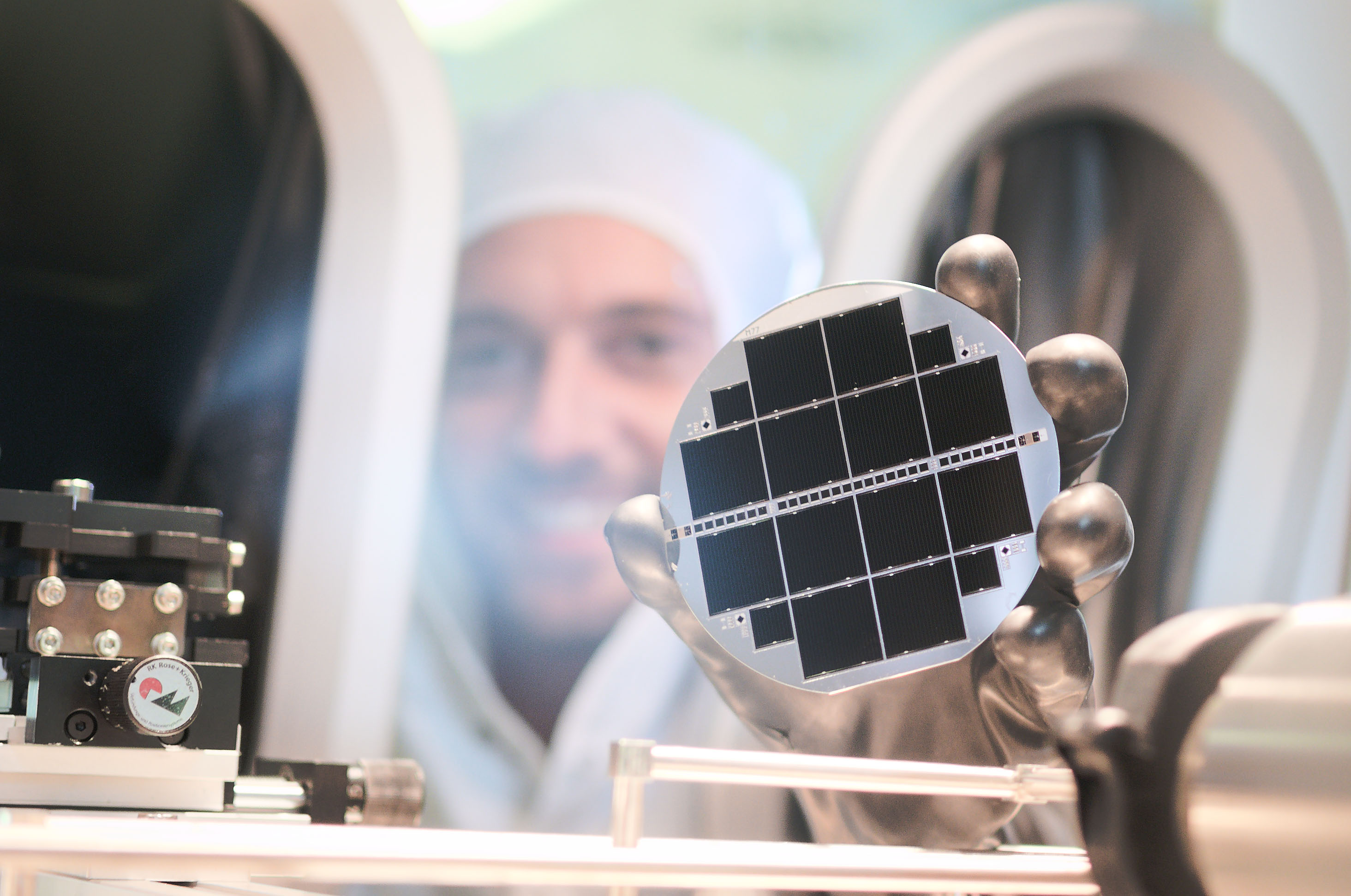
Researchers at the Fraunhofer Institute for Solar Energy Systems ISE have succeeded in raising the efficiency value of monolithic triple-junction solar cells made of silicon and III-V semiconductor materials.
Using a combination of multiple absorber materials, these multi-junction photovoltaic cells exploit the energy from the solar spectrum significantly better than conventional silicon solar cells. The world record for a monolithic multi-junction solar cell manufactured by wafer bonding has been increased to 34.1 percent and an efficiency record of 24.3 percent achieved for a solar cell with the III-V semiconductor layers deposited directly on the silicon.

Above: IV-characteristics of both of the new III-V semiconductor and silicon triple-junction solar cells, measured at Fraunhofer ISE CalLab PV Cells under AM1.5g standard test conditions. The cells each have an area of 4 cm2.
“Monolithic multi-junction solar cells are a source of hope for the further development of the silicon solar cells dominating the field today because they can lead to significantly higher efficiency values when converting sunlight into electrical power. We believe that we can achieve efficiency values of 36 percent, which would substantially exceed the physical limit of 29.4 percent offered by a pure silicon solar cell,” explains Andreas Bett, institute director of Fraunhofer ISE. The high efficiency allows for more output per surface area, thus creating a savings of solar cell and module materials — an important aspect in regard to the sustainability of photovoltaics.
For the production of multi-junction photovoltaic cells, thin III-V semiconductor layers only a few micrometers thick are deposited on a silicon solar cell. In order to optimally exploit the sun’s rays, the different layers absorb light from different spectral ranges: GaInP in the 300–660 nm range (visible light), AlGaAs in the 600–840 nm range (near infrared light) and silicon in the 800–1200 nm range (long-wavelength light). This enables significantly increased efficiencies compared to single-junction silicon solar cells. Like today’s conventional silicon solar cells, these cells each have a contact on the front and rear sides, which allows for easy integration in solar modules.
Bonded multi-junction photovoltaic cells: 34.1 percent efficiency
Already well established in microelectronics, the process of direct wafer bonding is employed for creating a monolithic multi-junction solar cell. This involves depositing the III-V layers on a GaAs substrate in an initial step, after which an ion beam is used to deoxidize the surfaces in a high-vacuum chamber before they are pressed together under pressure. The atoms in the III-V semiconductor layers form a bond with the silicon, forming a single unit. Now stacked on top of each other, the GaInP, AlGaAs and silicon sub-cells are interconnected via tunnel diodes. The GaAs substrate is subsequently removed using wet chemistry, a nanostructured rear-side contact is attached and an anti-reflection coating and a contact grid are applied to the front side.
“In contrast to earlier results, the deposition conditions were improved and a new cell structure was introduced for the uppermost sub-cell made of GaInP which enables even better visible light conversion than before. With an efficiency of 34.1 percent, the cell demonstrates the immense potential of this technology,” says Frank Dimroth, head of department III-V Photovoltaics and Concentrator Technology at Fraunhofer ISE. The former world record for this cell class was 33.3 percent efficiency.
Multi-junction photovoltaic cell with directly deposited semiconductor layers: 24.3 percent efficiency
Directly depositing the III-V semiconductor layers (GaInP/GaAs) on the silicon solar cells is another method used to create multi-junction photovoltaic cells. This procedure involves considerably fewer process steps than wafer bonding and avoids the use of expensive GaAs substrates, which means it is quite advantageous in the industrial implementation of this technology.
Nonetheless, the atomic structure must be very carefully controlled to ensure that the gallium and phosphorous atoms are arranged on the correct lattice sites at the interface to the silicon material. Defects in the semiconductor layers can also have an adverse effect on the solar cells’ efficiency. “We were able to make major progress in this area — current generation in the three sub-cells is now barely affected by these defects, which has enabled us to realise 24.3 percent efficiency for this technology for the first time anywhere in the world,” Frank Dimroth says. “The potential is comparable to that of the wafer-bonded cells. We’ve got our work cut out for us in the coming years in order to prove that this is the case.” In December 2018, Fraunhofer ISE introduced this type of solar cell with an efficiency record of 22.3 percent.
In heading toward the industrial mass production of monolithic multi-junction photovoltaic cells, Fraunhofer ISE researchers see challenges in particular in finding an affordable process for manufacturing the III-V semiconductor layers. Direct growth on silicon is currently the most promising approach, but other methods are being researched where the GaAs substrates can be recycled many times over after the semiconductors are transferred to the silicon. For cost-effective solar cell production new deposition machines with higher throughput and deposition area will be required. These are all methods that researchers at ISE will pursue in the coming years.
Work on wafer-bonded solar cells is funded by the German Federal Ministry for Economic Affairs and Energy (PoTaSi project, FKz. 0324247). Work on directly grown cells, in which partners Aixtron SE, TU Ilmenau and Philipps-Universität Marburg were involved, was funded by the German Federal Ministry of Education and Research (MehrSi project, FKz. 03SF0525A).


