
Mitsubishi announces First Multi-Cell GaN HEMT on diamond
Technology will improve the power-added efficiency of high-power amplifiers in wireless communication
Mitsubishi Electric has announced that in collaboration with the Research Centre for Ubiquitous MEMS and Micro Engineering, National Institute of Advanced Industrial Science and Technology (AIST), it has developed a GaN-HEMT in a multi-cell structure (multiple transistors cells arranged in parallel) bonded directly to a single-crystal diamond heat-dissipating substrate with high thermal conductivity.
The direct bonding of a multi-cell GaN-HEMT to a single-crystal diamond substrate is believed to be a world first. This research achievement was announced at the International Conference on Solid State Devices and Materials (SSDM) currently being held at Nagoya University, Japan from September 2 to 5.
The new GaN-on-Diamond HEMT has been designed to improve the power-added efficiency of high-power amplifiers in mobile communication base stations and satellite communications systems, thereby helping to reduce power consumption. Mitsubishi Electric will refine the GaN-on-Diamond HEMT prior to its commercial launch targeted for 2025.
Mitsubishi Electric handled the design, manufacture, evaluation and analysis of the GaN-on-Diamond HEMT and AIST developed the direct bonding technology. A part of this achievement is based on results obtained from a project commissioned by the New Energy and Industrial Technology Development Organization (NEDO).

Most existing GaN-HEMTs that use a diamond substrate for heat dissipation are created using a GaN epitaxial layer foil from which silicon substrate has been removed and onto which diamond is deposited at high temperature. HEMTs are then fabricated on the diamond substrate of the flattened GaN wafer. However, because the thermal expansion coefficients of GaN and diamond are different, the wafer can warp greatly during the manufacturing process, making it difficult to fabricate large multi-cell GaN-HEMTs.
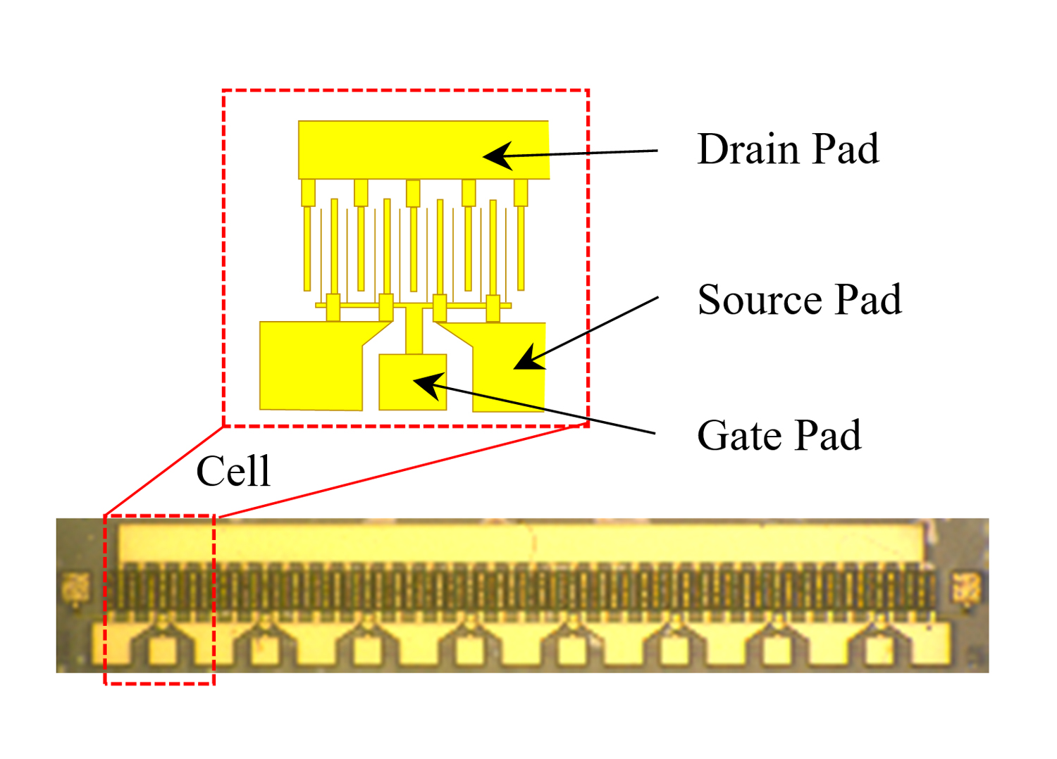
During this research a silicon substrate was removed from a multi-cell GaN-HEMT that was fabricated with a silicon substrate; the back surface of the GaN-HEMT was then polished to make it thinner and flatter, after which it was bonded directly onto a diamond substrate using a nano adhesion layer. A multi-cell structure was used for the parallel alignment of eight transistor cells of a type found in actual products. Finally, a multi-cell GaN-on-Diamond HEMT—the world’s first—was fabricated using a substrate with high heat dissipation made of single-crystal diamond.
Using a single-crystal diamond (thermal conductivity of 1,900 W/mK) for superior heat dissipation suppresses temperature degradation, decreasing the temperature rise of the GaN-HEMT from 211.1degC to 35.7degC. This improves output per gate width from 2.8 W/mm to 3.1 W/mm as well as raising power efficiency from 55.6 percent to 65.2 percent, thereby realizing significant energy conservation.
There are two completed patents for the technology and nine pending patents in Japan and ten patents pending outside of Japan.


