
BluGlass: Cascade LEDs and beyond
Working with Bridgelux, BluGlass intends to swiftly bring cascade LEDs to market. But this is just the beginning, reports Rebecca Pool.
In a move that marks the latest in a long line of developments this year, BluGlass has signed a joint development agreement with LED manufacturer, Bridgelux, US, to develop cascade LEDs.
The Australia-based developer of remote plasma chemical vapour deposition (RPCVD) will grow buried activated p-GaN layers on wafers, creating tunnel junctions that can be stacked to form cascade LEDs.
Bridgelux will work with BluGlass - as part of the none-exclusive agreement - to evaluate the low temperature, ammonia-free deposition process and tunnel junctions for cascade LEDs. And if all goes to plan, these LEDs will soon be ready for general lighting markets.
“We're taking wafers and growing materials on them using RPCVD, and Bridgelux is going to create and characterise devices, feeding back data to us,” says BluGlass managing director, Giles Bourne. “Our tunnel junction technology has come on in leaps and bounds in the last year and we can now move reasonably quickly on this.”

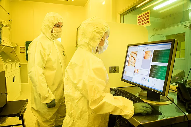
BluGlass and Bridgelux are relying on RPCVD to get cascade LEDs to market quickly. [BluGlass]
Industry-wide, cascade LEDs are regarded as a means to mitigate so-called efficiency droop by combining LEDs in a single, vertical stack and generating greater light output for less power. However, conventional MOCVD has, so far, failed to deliver the necessary tunnel junctions at commercial-scale as high temperature growth introduces impurities to epitaxial layers.
To achieve low temperature growth, BluGlass has been retrofitting the most common MOCVD systems in the market. The company replaces the ammonia source of an existing system with nitrogen gas, passed though an electrical coil to generate a plasma.
Directly supplying nitrogen via this plasma allows layer deposition at relatively low temperatures, which is crucial to the manufacture of practical GaN-based tunnel junction devices and cascade LEDs.
Earlier this year, the company patented its method to simply and swiftly fabricate the buried activated p-(Al, In) GaN layers so critical for tunnel junction function. As Bourne says: “Our process has unique properties so we can grow a very good tunnel junction.”
And working with Bridgelux, the managing director reckons devices could reach market within two to three years, “and hopefully a lot sooner”.
“Bridgelux has very a good front-end technology in terms of devices and combining this with our low temperature RPCVD is a good way of accelerating [cascade LEDs] into the market,” he says. “Having a partner with oodles of experience of manufacturing devices will help us to get to this endgame.”
But cascade LEDs and general lighting is only the first application that BluGlass hopes to reach with its tunnel junctions. As Bourne point out, the company has also been developing the technology for UV-LEDs, laser diodes and microLEDs.

X-Celeprint has used RPCVD p-GaN layers to develop an active matrix microLED display prototype. [BluGlass]
BluGlass is currently working with a Europe-based group on microLEDs. And in May this year, Ireland-based BluGlass foundry customer, X-Celeprint, unveiled an active matrix microLED display that uses RPCVD p-GaN layers. The prototype has delivered good luminance with colour uniformity, quantum efficiency and forward voltage that equals current high-performance commercial applications of high brightness, 2000cd/m2 displays.
Growing plans
To keep pace with the technology growth, BluGlass tripled capacity when it opened new manufacturing facilities - 'The Paul Dunnigan Labs' – at its Silverwater site, in August this year. Total investment exceeded $6 million, including the installation of two new reactors that brought the company's deposition system count to five.
A new BLG-300II RPCVD system, based on Aixtron's Thomas Swan 19 by 2 inch reactor, is already online. Meanwhile, a commercial-scale Aixtron 2800 G4 retrofit will be up and running by the end of this calendar year.
“As well as sapphire we have been doing a lot of work on silicon wafers and have a collaboration with a partner that exclusively uses silicon,” says Bourne. “We are wafer-agnostic and while the LED industry has been predominantly using sapphire, larger area silicon works well with our low temperature systems.”
Right now, the company largely deposits layers on two-inch wafers, but Bourne says scaling to 4 and 6 inch wafer sizes is not an issue. And while 8 and 12 inch wafers are more challenging, he highlights how systems are configured to handle these larger diameters.
BluGlass also hopes to continue collaborating with Aixtron. As Bourne says: “At the moment our [Aixtron] joint development agreement is really to support the architecture of the tools but in the longer-term we would like to see how [our technology] can fit into new tool-sets.”
“As a business we do not want to get into tool manufacturing... so Aixtron is looking at the technology and how it can be of commercial interest to the company later on,” he adds.
And looking to the future, Bourne is excited. “We've got a good baseline technology and I'm looking forward to turning all the hard work from the last decade into commercial output,” he says. “Ultimately this is about being part of someone's supply chain - that's what I am really excited about.”


