
Researchers integrate 2D semiconductor into a PIC
Scientists from Imec, Ghent University and MIT provide a promising route to scalable quantum photonics
Researchers from Imec's photonics research group at Ghent university and MIT have integrated a WSe2 monolayer onto a Silicon Nitride (SiN) photonic chip. They say the results, published in Nature Communications, provide a crucial step in fundamental quantum photonics and 2D materials research.
Photonic integrated circuits (PICs) enable the miniaturisation of complex quantum optical circuits connecting large numbers of photonic devices with optimised insertion losses and phase stability. A central building block for such an integrated quantum circuit is a single photon emitter (SPE), and a variety of material systems have been investigated to create such on-chip SPEs.
2D-semiconductor based SPEs have some unique properties that make them particularly appealing for integration with PICs. First, they can be easily interfaced with PICs and stacked together to create complex heterostructures. Second, due to their thinness, and the absence of total internal reflection, they enable very high light extraction efficiencies without the need of any additional processing, allowing efficient single photon transfer between the host and the underlying PIC. Third, 2D materials grown with high wafer-scale uniformity are becoming more readily available.
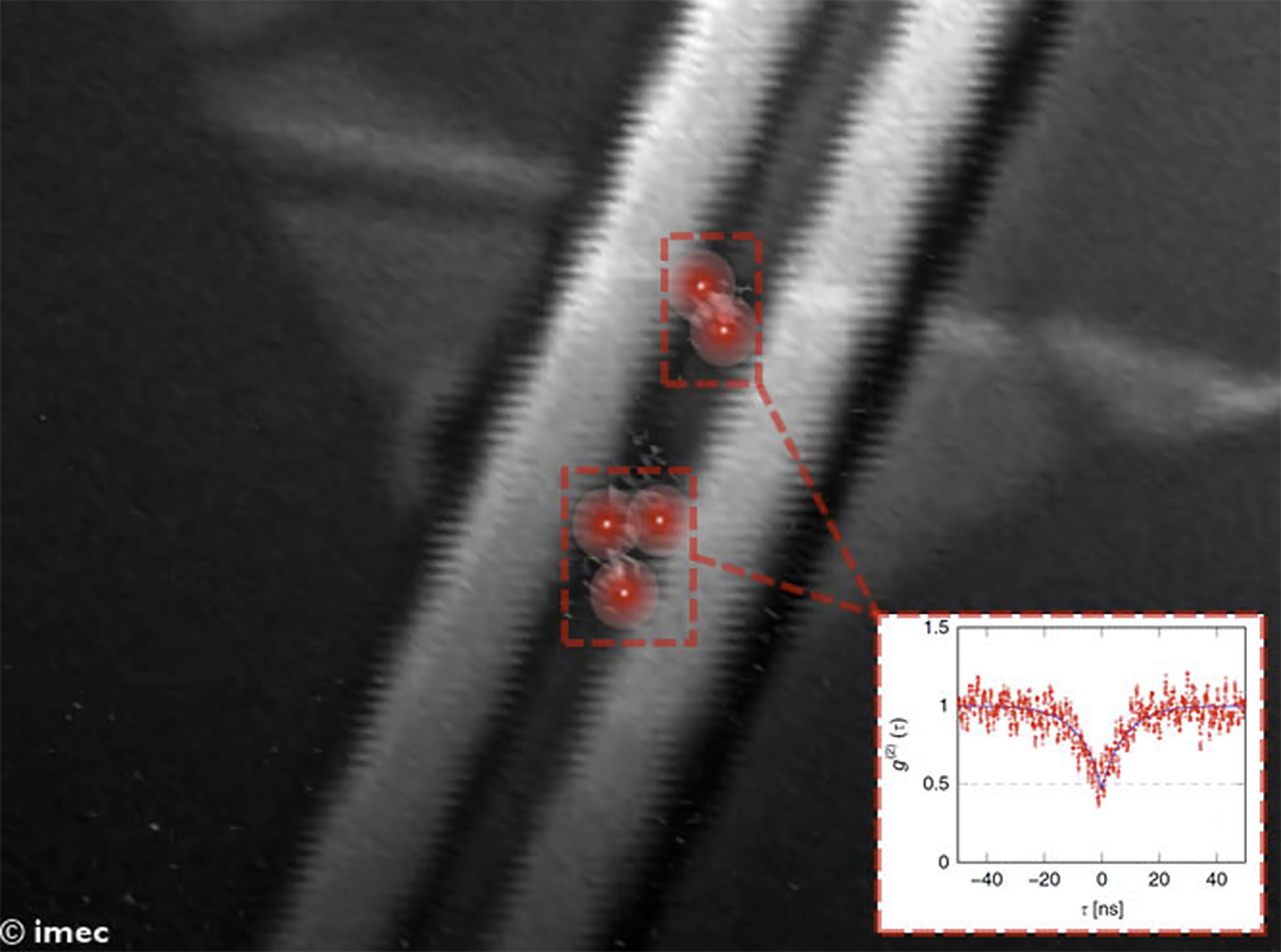
Through nanoscale strain engineering, the team coupled 2D-WSe2 based SPEs with a CMOS-compatible SiN waveguide. (The picture above shows the 2D monolayer on a SiN waveguide.)
Moreover, they extracted crucial performance parameters for this source and used them in an optimisation analysis to maximise single photon extraction and indistinguishability into the guided mode. They found that even for moderate quantum yields, dielectric cavities could be designed such that the single photon extraction into the guided mode can reach unity.
“These results provide a crucial step in scaling up quantum photonic devices using 2D-based integrated single photon sources,” said Frédéric Peyskens, first author of the paper.
'Integration of single photon emitters in 2D layered materials with a silicon nitride photonic chip' by Frédéric Peyskens et al; Nature Communications 10, Article number: 4435 (2019)


