Evaluating the substrate market

Richard Stevenson quizzes Yole Développement’s Hong Lin and Ezgi Dogmus on the state-of play on all the major compound semiconductor substrate markets, and what the future might hold for them.
Q: The Wolfspeed division of Cree has been making the headlines for exclusive wafer supply agreements. In the last year or so, it has signed a deal with Infineon that is worth over $100 million, one with STMicroelectronics valued at $250 million, and it has entered into two additional contracts, each worth over $85 million – one with ON Semiconductor, and the other is with an undisclosed power device manufacturer. What does this tell us about SiC substrate supply in this industry?
HL: The wafer is the key to the power SiC industry. There has been a shortage of supply in the market since 2016. Wolfspeed have invested significantly to produce their wafers. They have a dominant position, and they are quite likely to keep that position for at least the next two or three years, without any problems. They have some competitors, such as II-VI, and newcomers, such as GTAT and other players – but those players are not likely to take Wolfspeed out of the number one position.
Q: Is the quality of 6-inch SiC still lagging that of 4-inch SiC?
HL: We cannot generally say that it is lagging. It is player dependent. There are players that are able to produce very good 6-inch quality. I think we are in a transition to 6-inch, and 6-inch will be really dominant in the coming years.
The wafer quality is slightly different for diodes and MOSFETs. MOSFETs have more stringent requirements. When you are talking to suppliers, there are different qualities of wafers. There is premium quality and medium quality, and the lead times are different, pricing is different.
Q: What is the SiC substrate market worth today, and how fast will it grow in the coming years?
HL: If we are talking about the power electronics market, today the market size is more than $100 million. But SiC is not just used for power electronics. It is also used for GaN-on-SiC for 5G applications. Together, the market size is more than $150 million. In both these markets we see double-digit growth.
Q: With the rise of internet streaming, sales of BluRay players have fallen. Has this impacted sales of GaN substrates, which have provided the foundation for making lasers for BluRay players?
HL: Bulk GaN was initially used in lasers for BluRay players. The fall in BluRay sales has not been good news for makers of bulk GaN substrates. But GaN is still used for laser diodes in other applications. They are taking off, so there is a kind of balance.
At some point in time there was some hype about GaN-on-GaN LEDs. This technology was pursued by the US company Soraa. But I think that excitement has past.

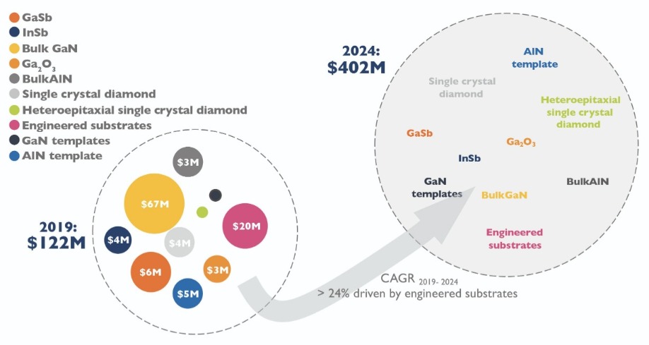
The total market revenue for emerging materials will more than triple between 2019 and 2024.
Q: There is interest in GaN substrates for making vertical GaN-on-GaN power devices. Has this translated into sales yet?HL: I don’t see any real commercial product. There is a lot of research, an increasing number of patents, and an increase in discussions about this at conferences. But we are still in the early phase of GaN-on-GaN power technology. If we compare to SiC, GaN-on-GaN is at least ten years behind.
Q: Does Sumitomo still dominate the market?
HL: The market is dominated by Japanese players. Not only Sumitomo Industries, but also SCIOCS and Mitsubishi Chemical.
Q: Do you think that the ammonothermal growth method for GaN will make a commercial impact? The Polish-firm Ammono failed to enjoy significant success but the Californian company Six Point Materials has high hopes?
HL: Ammono went into bankruptcy, but they have been taken up by the Polish Institute of High Pressure Physics. So it’s not 100 percent closed – there is still some pilot-line capability. Six Point have started to make 2-inch material. Development will take time.
Q: There is much interest in ultra-wide bandgap materials, including AlN and gallium oxide. I understand that AlN is incredibly difficult to produce. Are there any significant commercial suppliers?
HL: For AlN, there is commercial product. There are 2-inch wafers available from Hexatech in the US. There are start-ups acquired by Japanese companies, and they have commercial products. There are 2-inch commercially available materials, but AlN remains a small market as of 2019 in our understanding.

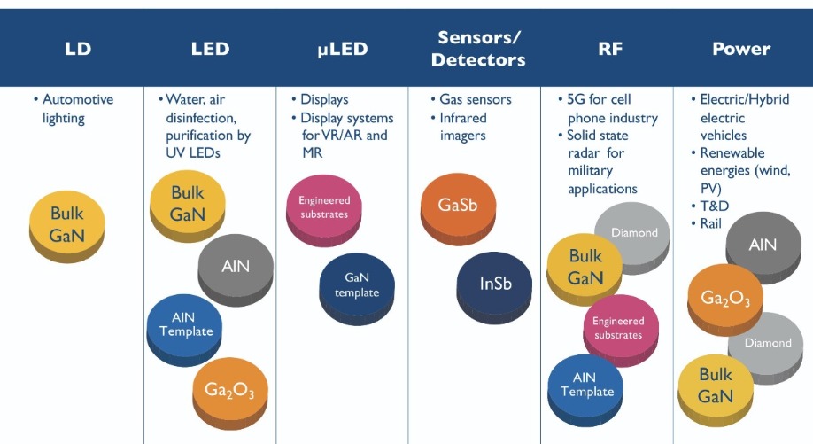
Over the next five years, markets will grow that offer new opportunities to a range of compound semiconductor substrates.
Q: For gallium oxide, crystals can be produced using established growth methods. How mature is this market, and who are the biggest players?HL: For gallium oxide, we have ten to fifteen years of delay compared with SiC in power electronics applications. Of course, gallium oxide has a lot of application possibilities.
I think the biggest player is Tamura. Novel Crystal Technology is there spin off. The closest to commercialisation at the device level is the Japanese start-up Flosfia. And you have development in the US, particularly for military applications.
Gallium oxide is still very far from commercialisation. But like vertical GaN, if you look at the number of publications per year, or the number of patents, they are increasing. I would not be surprised if in two or three years we will see a lot of start-up companies providing wafers. At the beginning of a new material, there will be a lot of small companies. If we look at the device level, diodes or MOSFETs, the progress is very significant over the last five years.
Q: What is the primary use for GaAs substrates? Is it to make the power amplifiers for mobile phones?
ED: One of the main applications for GaAs is the power amplifiers in mobile phones. We hope to see GaAs in 5G phones, so it will still have its position in the RF industry.
Q: Is there much demand for GaAs substrates for LEDs, lasers and solar cells?
ED: We see for the LEDs, the GaAs market is quite big. With GaAs, the bandgap is quite suitable for red and infrared applications. In the large display technologies, you see GaAs being used for red LEDs. This is a domain that is emerging, because you need more resolution, so you need smaller LEDs, and more and more LEDs in a display. So it will increase, a lot, the GaAs LED market.
We also see the laser market going up for GaAs. You will have heard of Apple using the GaAs VCSELs – the vertical-cavity, surface-emitting laser. They are used for 3D sensing, for facial recognition. This has produced a big change in market dynamics. Instead of more GaAs [edge-emitting] lasers, we see more Android users adopting this solution.
For the solar cells, the market is still small. A long time ago there was hope for GaAs for high-efficiency solar cells. But in the beginning of 2010s, we saw silicon solar cells decrease a lot in price, and the competition has become very tough. That’s the smallest market for GaAs substrates today.
Q: I understand that there has been a substantial fall in the average selling price of GaAs substrates over the last few years. Is that correct?
ED: The average selling price is application dependent. For RF, which is a big, stable market, we do not see a big decrease in the ASP. It is a similar situation for the LED. But for the VCSEL, there will be some price erosion over the next few years, because there is a big interest in this domain, due to 3D sensing and other VCSEL applications.
Q: Who are the leading suppliers of GaAs substrates?
ED: There are three big suppliers of GaAs substrates: the German company Freiberger; Sumitomo of Japan; and the US company AXT, which is also based in China.
Q: What are the most popular diameters for GaAs substrates?
ED: It is application dependent. For RF, for power amplifiers in handsets, it is 6-inch. For LEDs, we see more 4-inch. With VCSELs, we see a transition to 6-inch, and we think it will stay at 6-inch.
HL: For GaAs, the wafer quality is application dependent. Chinese players are developing material for the low-end, for LED applications. The market share, in dollars, is small, but the volume could be quite high.
Q: For InP substrates, are telecom lasers the biggest application?
ED: For lasers, the biggest applications are telecom and datacom. Increases in volume are driven by datacom applications, with Google, Amazon and other players implementing data centres. For telecom applications, this market is also increasing. As volumes are increasing, we are expecting the price to fall.
Q: Which companies are dominating the InP substrate market?
ED: There is AXT, Sumitomo and JX Nippon. They are the top three players.


