
InP DHBTs eye millimetre-wave 5G

Optimised InP DBHTs deliver the high breakdown and the low knee-voltage required for high-efficiency 5G power amplifiers
BY Yuefei Yang, Dheeraj Mohata, Dave Rasbot, Ricardo Soligo and David Wang FROM Global Communication Semiconductors AND Robert Bayruns, John Bayruns, David Osika and Joseph Brand FROM Duet Micro Electronics
The 5G network will roll-out in two phases. The first of them, involving frequency bands below 6 GHz, is already being deployed in several cities in different countries. Following in several years will be the second phase, offering higher data rates, greater capacity, better quality and lower latency.
Deployment of the second phase involves the introduction of frequencies within the millimetre-wave Ka-band that spans 24 GHz to 40 GHz. These higher frequencies will enable the delivery of multi-gigabit speeds to homes, apartments and businesses, in the form of millimetre-wave fixed wireless access, featuring phase-array beam-steerable active antennas and massive MIMO (multiple inputs, multiple outputs).
Throughout the evolution of wireless technologies, the power amplifier (PA) has been a critical component within the active antenna of every connected device. In today’s 3G-4G LTE market, the dominating technologies for this form of amplifier are the GaAs HBT and silicon LDMOS. The former offers performance, as well as flexibility of manufacturing, while the latter majors on maturity, low cost and a high level of integration.
At millimetre-wave frequencies, neither of these technologies is expected to fulfil the performance requirements, due to inherent material limitations. More promising are the 0.15 µm GaN HEMT, the 0.15 µm GaAs pHEMT, the micrometre InP DHBT, and nanoscale silicon CMOS and SiGe BiCMOS technologies.
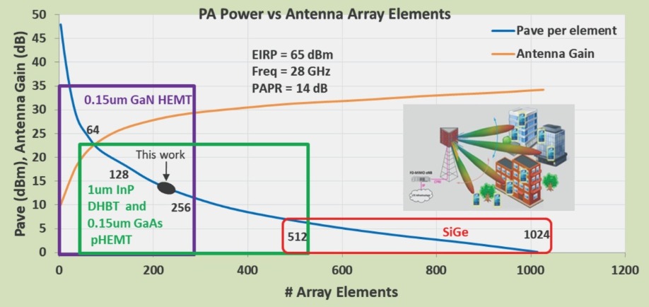
Figure 1. The required PA power and antenna gain for a varying number of antenna elements. GaN HEMT and InP DHBT PAs need fewer antenna elements, due to their high power capability; while SiGe BiCMOS need more elements, due to their low power capability.
Power amplifier considerationsEfforts are underway to determine the best design for the active antenna array elements in 5G millimetre-wave fixed wireless access systems. For the antenna, the effective isotropic radiated power (EIRP) is typically 65 dBm. This target can be met in many ways – it can be fulfilled with a small number of high-power PAs, such as those formed with GaN HEMTs; or it can be met with far more lower-power PAs, like those made from silicon CMOS or SiGe BiCMOS (see Figure 1 for an overview of various options). Note that selecting a large number of antenna elements with silicon CMOS or SiGe BiCMOS could result in a more expensive, less efficient solution.
A useful rule of thumb is that if a given technology is to be useful at a given frequency, its maximum oscillation frequency for power gain, a metric known as fmax, must be at least four times its operational frequency. So, for operation at 28 GHz, fmax should be 120 GHz or more.
There are several downsides to using HEMTs for amplification at these frequencies. Whether made from GaN or GaAs, the gate length must be no more than 0.15 µm. In compound semiconductor fabs, such a short gate length tends to be reached with electron-beam lithography, which is often a very high-cost, low-throughput solution. Another issue is related to the operation of the HEMT. To realise a high power, it must be driven with a high supply voltage, and withstand a high breakdown voltage. Realising very high breakdown voltages and delivering very high powers are well within reach of the GaN HEMT, but this transistor – and also the GaAs D-mode pHEMT – requires negative supplies for the gate bias, and the inclusion of a device that acts as a drain cut-off switch. These additions contribute to cost and complexity. And on top of these drawbacks, HEMT technologies intrinsically suffer from poor linearity and a low power-efficiency.
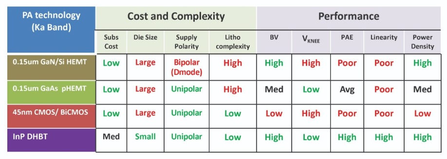
Table I: Manufacturing cost, complexity and performance comparison between PAs from competing technologies for 5G Ka-band millimetre-wave applications.
A promising alternative to the HEMT is the InP DHBT. It is renowned for its high speed, high linearity, high power efficiency and low off-state leakage current – a set of attributes that are highly desired for handset applications. Short gate lengths are not an issue, as the minimum feature size can exceed 1 µm, making this device easy to manufacture with high throughput in any III-V fab.One of the concerns with the InP DHBT is the high cost associated with both the substrate and the epitaxial process. Although InP substrates are needed for making lasers, the devices are very small, so substrate volumes are not substantial. But they could be, leading to lower prices, if production of the InP DHBT takes off.
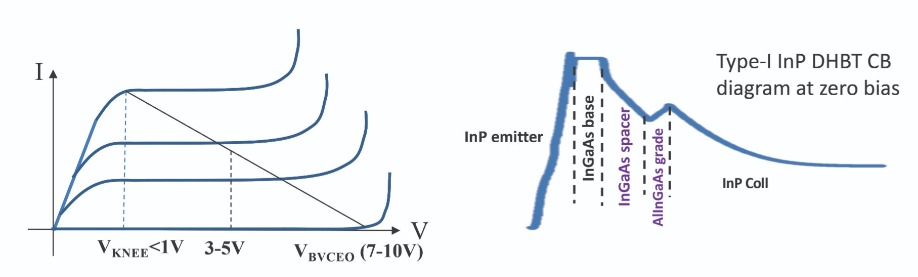
Figure 2. (Left) Output family of current-voltage curves for a power transistor showing the desired knee-voltage (VKNEE) and breakdown voltages to maximise the output power while maintaining good efficiency. (Right) Conduction band diagram showing the presence of a barrier between an In0.53Ga0.47As base and an InP collector. Spacer and grading layers smooth out the band-discontinuity and move it away from the junction.
Another challenge is that when the InP DHBT targets millimetre-wave PA applications, it tends to be compromised by the low collector-to-emitter breakdown voltage, BVCEO. This stems from the use of un-optimised narrow bandgap InGaAs in the base-collector junction.At Global Communication Semiconductors LLC, working in partnership with a team from Duet Micro Electronics, we have addressed the low breakdown voltage in these devices. Our success comes from optimising the transition layers in the base-collector junction by fine-tuning the doping and the thickness. This has enabled the production of InP DHBTs with a level of performance that makes them an attractive candidate for 5G networks.
Increasing the breakdown voltage
During the typical operation of a power amplifier, the output voltage swing peaks at twice the operating voltage. So, in cellular applications where the operating voltage is often between 3 V and 5 V, output voltage swings can hit 10 V. Ideally, this requirement is met while ensuring that the knee-voltage is below 1 V at a collector current density of more than 100 kA cm-2, as this allows the output power to be maximised while drawing on the full benefits of envelope tracking (see Figure 2, left).
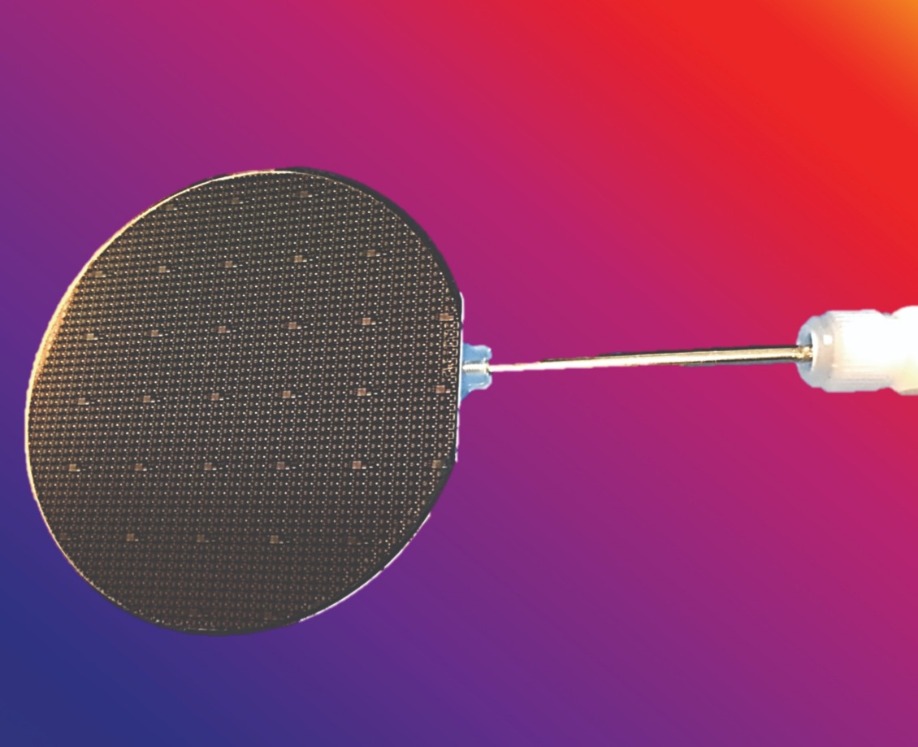
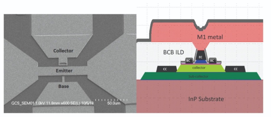
Figure 3. (Top) Processed 4-inch InP DHBT wafer, held using a vacuum wand. (Bottom left) Tilted view scanning electron micrograph showing metal 1 routing to the base, collector and emitter contacts of the DHBT. (Bottom right) Cross-section of a typical GCS InP DHBT.
The key to meeting all these requirements is to optimise the base-collector junction. The type I band alignment between the In0.53Ga0.47As and InP layers creates a significant energy barrier for electrons transiting from the base to the collector (see Figure 2 right). Normally, in this region of the device there is an In0.53Ga0.47As spacer and a quaternary grading layer made of an InAlGaAs alloy, a combination that smooths out this discontinuity or moves it away from the base-collector junction. The trick is to choose the right combination of thicknesses and doping, to ensure good trade-offs between: the unity gain cut-off frequency, fT; the maximum oscillation frequency, fmax; the breakdown voltage, BVCEO; and the knee voltage, VKNEE.By improving the design of the epilayers in our InP/In0.53Ga0.47As DHBT, we have increased the BVCEO of our transistors to around 11 V. Devices with this level of ruggedness have been made by processing 4-inch InP epiwafers, produced by solid-source MBE (see Figure 3 for an image of the processed wafer, along with a tilted-view scanning electron microscopy image of the fabricated DHBT, and a cross-sectional diagram of the DHBT, including the contact layers).
We have measured the collector-emitter leakage curves of our transistors, along with their output current-voltage characteristics (see Figure 4). Collector-emitter breakdown behaviour is abrupt, implying that the material has reached its intrinsic breakdown. The knee voltage is low, measuring just 0.6 V at a collector current density of 120 kA cm-2.
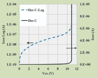
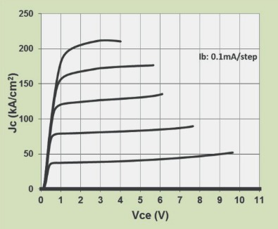
Figure 4. (Left) Iceo verses Vce for optimised InP/In0.53Ga0.47As DHBT epi design. Device size is 1.6 µm by 10 µm. The collector-emitter junction achieves sharp breakdown and low leakage. (Right) Output current-voltage curves show low knee-voltage characteristics.
The high-frequency performance of our transistors is very encouraging. We have measured an fT of 115 GHz and an fmax of 150 GHz (see Figure 5).These values, plus those for the breakdown voltage and the knee-voltage, indicate that our InP DHBT is a very good device for Ka-band operation.
A two-stage amplifier
Drawing on our optimised DHBT, we have designed and fabricated a two-stage power amplifier (see Figure 6 for images). Die size is just 0.7 mm by 1.2 mm, making our amplifier far smaller than other technologies – a valuable trait given the premium placed on a small footprint inside the smartphone. Within the circuit there is a CMOS compatible-current mirror, which supplies a reference current to the first and second stages. To minimise the effects of through-wafer via inductance, the output stage is divided into four power-cells, combined at the inputs and outputs.
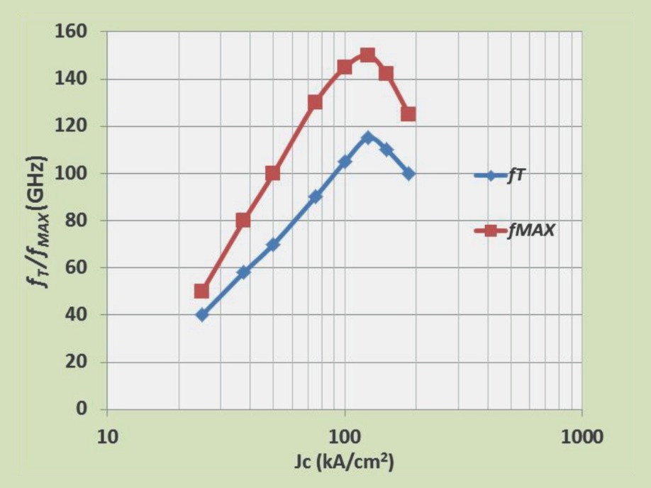
Figure 5.fT and fmax versus the collector current density, Jc, for a DHBT with emitter size of 1.6 µm by 10 µm. Maximum fT of 115 GHz and maximum fmax of 150 GHz are obtained.
Measurements on this amplifier, run at an operating voltage of 3 V, show a gain of about 18 dB between 27.5 GHz and 28.35 GHz (see Figure 7, left). At this operating voltage, a power sweep at 28 GHz reveals a saturated power, PSAT of about +26 dBm when the circuit is driven 5 dB into compression. At this condition, the measured power-added efficiency, PAE, is 54 percent (see Figure 7, right).These measures of performance allow us to determine the number of elements in an array. The good news is that this figure is 256, far less than the number required for silicon CMOS or SiGe BiCMOS technologies. And simulations suggest that an even lower number is possible. Increase the operating voltage to 5 V, the PSAT is expected to hit 30.4 dBm, allowing the number of elements to fall to a more usable 128 (see Table 2 for a detailed evaluation of our technology, compared with 45 nm SOI CMOS, 0.13 µm SiGe BiCMOS, 0.15 µm GaAs pHEMT and 0.15 µm GaN HEMT).
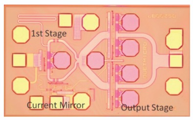
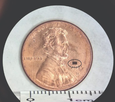
Figure 6. (Left) Optical micrograph of a two-stage power amplifier using InP DHBTs. (Right) Comparing die size to that of a nickel dime. Die size is 0.7 mm by 1.2 mm. In this amplifier, the first stage input has a bandpass match topology; the inter-stage match is low-pass as well as the final output match.
Another encouraging sign for our technology relates to the plots of S21, the power transferred from port 1 to port 2. We have measured this figure for about 100 die across a 4-inch wafer. Results highlight good PA performance uniformity across our wafer.Our work makes a strong case for the InP DHBT millimetre-wave PA in fixed wireless access and handset applications. It’s not just that the overall PA performance is better; the process is simpler, and the chip size is smaller than rival technologies. What’s more, it offers a single supply voltage, and the low power-down DC leakage current for the InP DHBT PA is especially attractive for handset applications.
So far, we have made PAs that use an emitter with a device size of 1 µm by 10 µm. We plan to progress to a larger optimum device size as we strongly believe that this will deliver further improvements in the performance of the PA, including a hike in the output power. This will get an additional boost by upping the operating voltage to 5 V. To assess the extent of these benefits, we are currently preparing to run a ‘design-of-experiments’ programme.
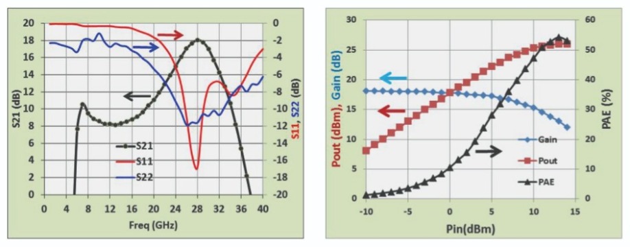
Figure 7. (Left) Measured S-parameters as a function of frequency. S21 is 18 dB at 28 GHz. The input match provides an S11 from -17 dB to -12 dB, while the output S22 is better than -10 dB across the band, indicating good matches for both input and output stages. (Right) Power sweep results showing power-added efficiency of 50 percent and a saturated power output of 26 dBm for a two-stage PA. Backed-off, the P1dB is +24 dBm.
Our efforts are also being directed at evaluating InP DHBTs that are grown on lower-cost substrates, such as GaAs or silicon. We want to determine if it is possible to maintain the performance of the PA with substrates that are lower in cost and less brittle.A third goal for our team is to carry out extensive reliability studies. Demonstrating the reliability of our InP DHBT will allow it to win substantial orders in Ka-band PA applications, and ultimately provide the best solution for millimetre-wave 5G networks.
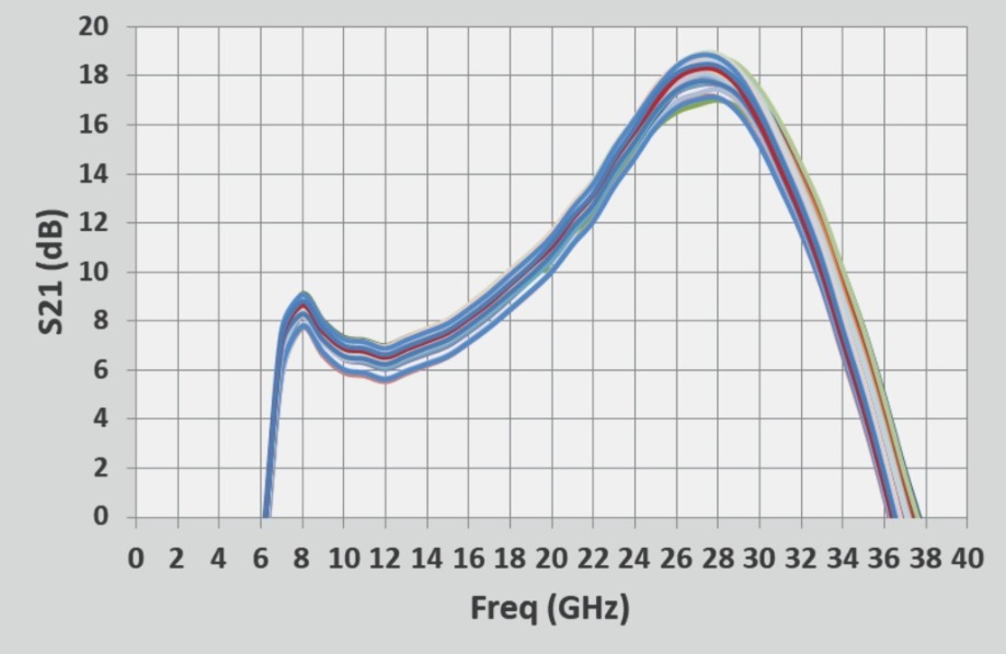
Figure 8. On-wafer S21 curves at multiple sites across a 4-inch wafer showing good uniformity.
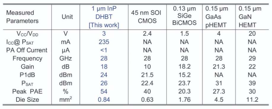
Table II: Summary of the two-stage PA of this work and comparison with other technologies.
SNS Telecom. “5G for FWA (Fixed Wireless Access): 2017-2030-Opportunities, Challenges, Strategies & Forecasts
D. Schnaufer et al. “Delivering 5G mmWave fixed wireless access” EDN, September 2017
Y. Yang et al. “Development of InP DHBTs with High Breakdown Voltage for Ka-Band PA Applications”, International Conference on Compound Semiconductor Manufacturing Technology, Minneapolis, MN, 2019.


