
Obliterating the thermal barrier in GaN-on-GaN devices
Thermal analysis reveals that backside processing reduces the rise in the temperature of GaN-on-GaN devices
BY NAOYA OKAMOTO FROM FUJITSU LIMITED AND FUJITSU LABORATORIES
The GaN HEMT is renowned for delivering a high RF output power at a high efficiency. Thanks to these qualities, this class of transistor can dramatically improve the performance of microwave to millimetre-wave radio communications and radar systems. These HEMTs could be used in weather radar systems, monitoring and predicting local heavy rainfall, and in 5G systems, providing communication in the millimetre-wave band.
Yet another opportunity for the GaN HEMT is as a successor to the conventional magnetron, providing heating in microwave ovens. This modification would usher in an era of innovative, compact microwave heating. Turning to HEMTs would suppress wasteful energy consumption by irradiating only the heating region with microwave energy.
The majority of commercially available RF GaN-based HEMTs are fabricated on SiC substrates. Using this foundation, the crystal quality of GaN is higher than it is for growth on sapphire and silicon, while the substrate combines a high thermal conductivity with excellent insulation (see Table 1 for a more detailed comparison of different substrates for GaN).
Efforts are underway all across the world to drive the output power and efficiency of the GaN HEMT to a new high, because this would lead to further improvement in system performance. That’s not easy, though, as GaN HEMTs are plagued by current collapse, which significantly diminishes drain efficiency. The primary cause of this malady is electron trapping, taking place at the buffer layer and at the interface between GaN and the passivation film, typically SiN (see Figure 1). A root cause of this issue is the high density of dislocations in the buffer layer, arising from growth on lattice-mismatched substrates.
An effective approach for quashing the dislocation density is to grow the epilayers on freestanding GaN. This substrate, which has a dislocation density of the order of 106 cm-2 or less, enables a reduction in the dislocation density of the GaN epitaxial layer by at least two orders of magnitude compared with the SiC substrate.
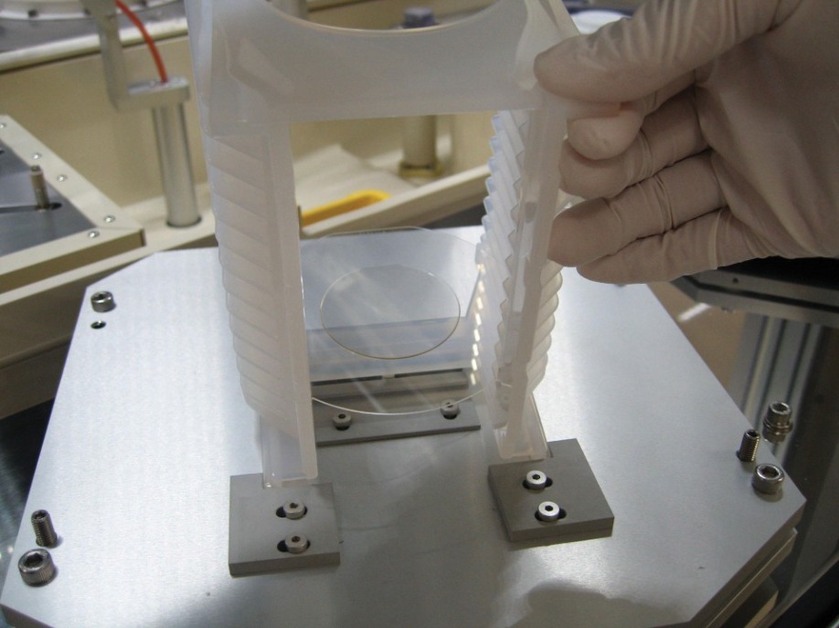
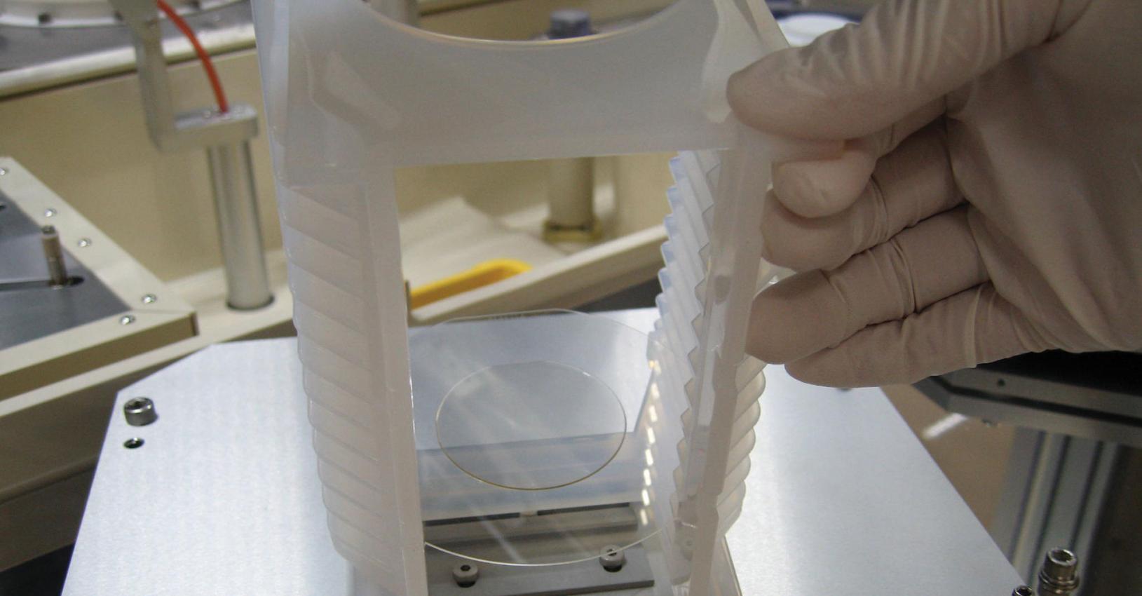
2-inch GaN substrate bonded to a 4-inch sapphire carrier and loaded into a grinder
Until recently, switching to a GaN substrate has not been that attractive, due to its high electrical conductivity. But recently this has changed, now that iron-doping has enabled the production of semi-insulating GaN. Although substrates are small – their diameter is just 2-inch – they can reduce the extent of current collapse considerably.The Achilles heel of the GaN substrate is its low thermal conductivity. At 230 W m-1 K-1, it is almost half of that for SiC. This is a significant weakness, as it leads to a degradation of device performance and reliability. The problem is particularly acute when HEMTs are used for microwave heating, because this requires continuous operation of the device, and increases the extent of heat radiation.
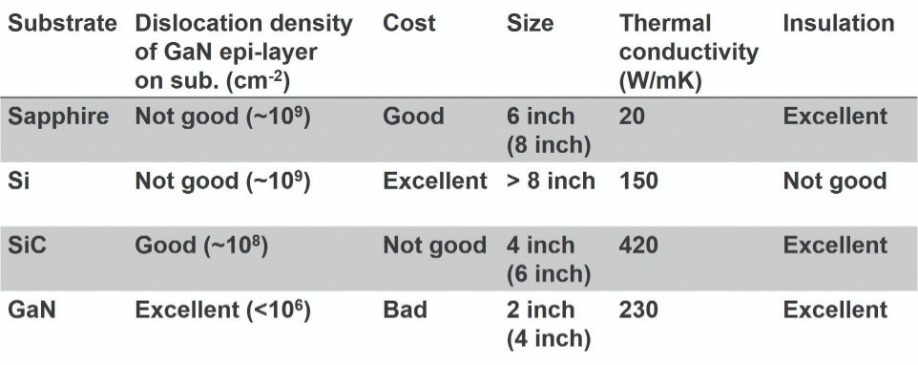
Table I. Comparison of substrates for GaN-HEMTs.
Tackling this issue is our team from Fujitsu and Fujitsu Laboratories. Recently, using insights from thermal analysis, we have shown that backside processing can improve the thermal management of this device.Thermal simulations
To optimise the thermal management of GaN-on-GaN devices, we begin by simulating a lateral HEMT with an output of tens of Watts. The merit of this approach, rather than an iterative one based on prototyping, is that it can quickly determine the best device structure and subsequent processes.
Before we started our simulations, we measured the thermal conductivity of semi-insulating GaN (0001) substrates grown using the void-assisted separation method by HVPE. Using the periodic heating method, we determined a thermal conductivity for the semi-insulating GaN substrate of 237 W m-1 K-1. This value is in good agreement with recent measurements from other groups.
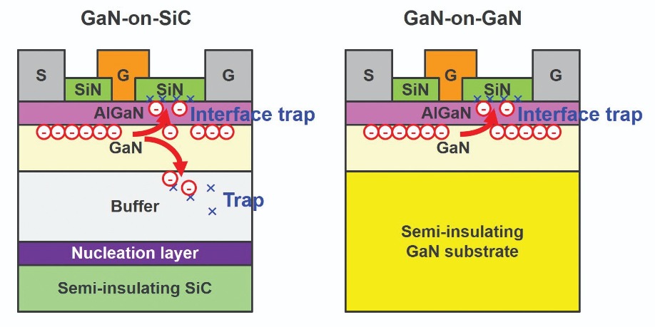
Figure 1. The cross-sections of typical GaN-on-SiC and GaN-on-GaN HEMTs.
Our simulations considered a GaN epilayer on a native substrate, which has a backside coated with a layer of AuSn, attached to copper (see Figure 2(a)). In a HEMT, most of the heat is generated at the drain-side edge of the gate electrode, where the electric field concentration peaks. To try and replicate this scenario, we introduce heat sources, with dimensions chosen to match the gate electrode size. Each heat source has a power that is equivalent to a 10 W/mm HEMT, operating with an efficiency of 58.8 percent. We vary the width of these sources, but fix their length and height at 0.5 µm and 0.1 µm, respectively. In our simulations, these sources are placed on top of a GaN epilayer, and we vary the spacing between them, along with their number.To ensure that our simulations are as realistic as possible, we account for the differences between growing GaN on its native substrate and on SiC. Growth of GaN-on-GaN ensures lattice matching, so there is no need for an AlN nucleation layer, and we can assume that the dislocation density in the GaN epilayer is as low as that in the GaN substrate. Based on these considerations, we adopt an extremely low value for the interfacial thermal resistance between the epilayer and the substrate – we use 1 × 10⁻¹⁰ m2 K W-1 – and we set the thermal conductivity of the GaN epilayer to 230 W m-1 K-1, which is approximately equal to that for the GaN substrate.
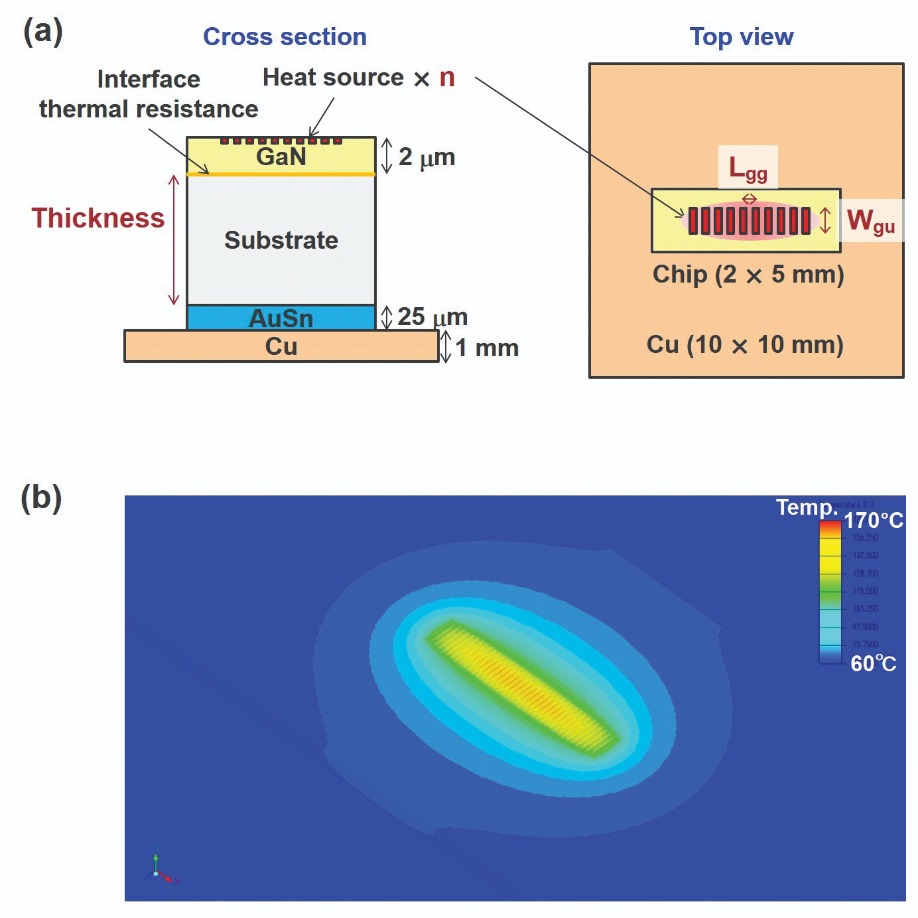
Figure 2. Simulated structure of a GaN-HEMT power amplifier (a) and an example of simulated thermal distribution (b).
With GaN-on-SiC, simulations are markedly different. When GaN is grown on SiC, an AlN nucleation layer is often inserted between the buffer layer and the SiC substrate. Another key difference is that the dislocation density of the GaN epilayer is about two orders of magnitude higher than that of GaN-on-GaN. To capture all of this in our model, we select a much higher value for the interfacial thermal resistance – we use 2.5 × 10⁻⁸ m2 K W-1 – and we reduce the thermal conductivity of the GaN epilayer to 130 W m-1 K-1. To determine the temperature rise, we calculate the difference between the maximum temperature of the simulated thermal distribution and the copper heatsink, held at 60 °C (see Figure 2 (b)).We have found that for a heat source spacing of 30 µm, thinning the GaN substrate to just 100 µm minimises the temperature rise (see Figure 3(a)). Note, however, that as the width of the heat source increases, the temperature rise of GaN-on-GaN can overtake that for GaN-on-SiC. This indicates that GaN-on-GaN can be easily filled with heat.
Is this a concern? Although at first glance it would seem to be, we have demonstrated that GaN-on-GaN has a higher thermal management potential than GaN-on-SiC. When the heat source spacing exceeds 40 µm, the temperature rise for GaN-on-GaN is suppressed more than that for GaN-on-SiC (see Figure 3(b)).
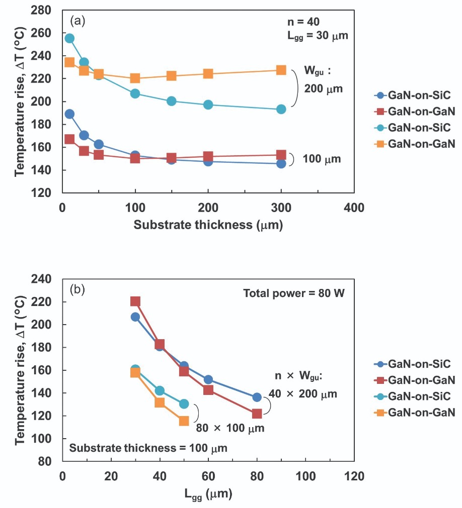
Figure 3. Simulated comparison of the temperature rise between GaN-on-GaN (§) and GaN-on-SiC(); (a)substrate thickness dependence, (b)gate-to-gate spacing distance dependence.
To understand why this is the case, one needs to consider the heat transfer mechanisms at play. When heat sources are less than 30 µm apart, the heat that is generated interferes in the GaN epilayer. From here, heat transfers to the substrate and spreads in a direction parallel to the heat sources (see Figure 4(a)). In this case, a SiC substrate is preferable to one made from GaN, because it has a higher thermal conductivity.A different conclusion is drawn when the spacing between the heat sources exceeds 40 µm. In this regime, thermal interference decreases, and it is effective to spread the heat in the GaN epilayer between the sources (see Figure 4(b)).
Where does the cross-over between the two modes of operation occur? Well, when the spacing between the heat sources is more than one-third of their width, GaN-on-GaN offers better heat dissipation than GaN-on-SiC, thanks to the higher thermal conductivity of the GaN epilayer.
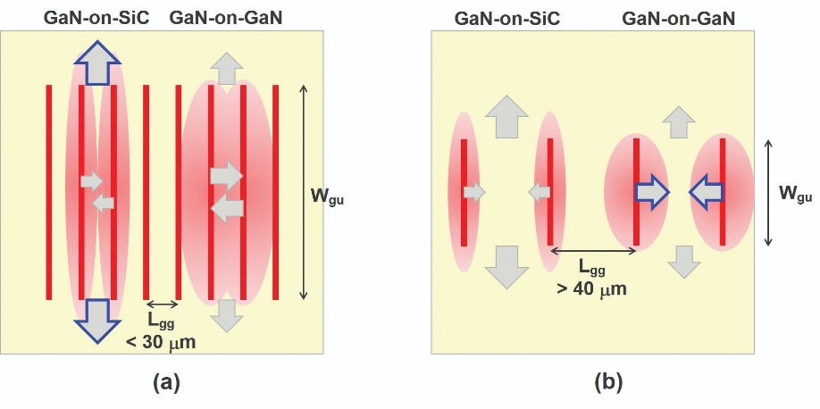
Figure 4. Difference in heat transfer mechanism, as viewed from the top of the device.
This finding has implications for many different GaN-on-GaN architectures. It should influence those developing lateral GaN-on-GaN HEMTs, and also those making vertical GaN devices. These results have motivated our team to develop a GaN substrate thinning process, to aid heat dissipation in GaN-on-GaN HEMTs.Backside processing
In general, GaN substrates are less sensitive to hardness than those made from SiC. Consequently, we can use our SiC through-substrate via-hole (TSV) process when backgrinding our GaN substrates. To undertake this, before we start backgrinding, we attach a 2-inch GaN substrate to a 4-inch sapphire support carrier with an adhesive.
The results of our thermal simulations have led us to target a thickness for the processed GaN substrate of less than 150 µm. We realise this in two steps: we begin by using a coarse grinder, which removes material at a rate of about 25 µm/min; and then we finish with a fine grinder, working at a rate of 1 µm/min. Using this approach, the total time for grinding is only about 15 minutes.
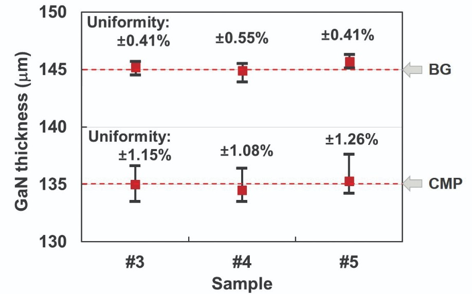
Figure 5. Thickness of the three processed GaN substrates after backgrinding (BG) and chemical-mechanical polishing (CMP).
Backgrinding realised a target thickness of 145 µm and an excellent thickness uniformity – it was within ± 0.6 percent (see Figure 5). We processed three of these thinned wafers, a task that suggests that we have a stable, controllable process. Atomic force microscopy uncovered typical scratches in the surface. We found that at the centre of the wafer, the grinding marks are random, but at the top, these marks are aligned in one direction. Based on the scan of a 2 µm square, average surface roughness is less than 2 nm.Unfortunately, backgrinding causes cracks in the wafer edges (see Figure 6(a)). This is an issue that never arose when grinding SiC. We attribute this problem to the GaN substrate being more brittle than SiC, and the wafer edge becoming knife-shaped, due to backgrinding. There is no cause for alarm, as we can eliminate the crack by trimming the wafer’s edge.
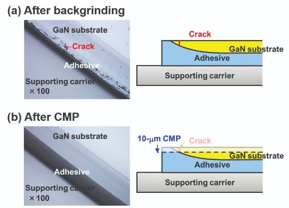
Figure 6. Photograph and schematic cross-section of wafer edge after backgrinding (a) and chemical-mechanical polishing (CMP) (b).
To improve the finish of our backgrinded GaN, we use a chemical-mechanical polish. No scratch marks remain after polishing for 2 hours with a silica-based slurry. This process removed a further 10 µm of the GaN substrate (see Figure 5) and eradicated the wafer edge cracks (see Figure 6(b)). Polishing did compromise the thickness uniformity of the GaN substrate – it increased to just below ± 1.3 percent – but it is still sufficient for the task in hand. Of greater significance is the improved surface morphology, with average surface roughness slashed to just 0.2 nm or less (see Figure 7).We also investigated a range of slurries. By refining our selection, we were able to trim the processing time by two-thirds. This time saving helps to reduce the time taken to produce GaN-on-GaN devices. In addition, we have recently increased our expertise, and can now control the thickness of the GaN substrate produced by backgrinding and chemical mechanical polishing down to 100 µm.
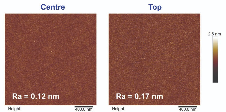
Figure 7. Atomic-force microscopy images of a GaN substrate after chemical-mechanical polishing.
During the polishing process, we identified larger micropipes, with a typical diameter of 160 µm. Some of these result from the exposure of embedded micropipes by the polishing process. However, the majority originate from polishing itself, which causes an expansion of dislocation defects. In the GaN substrates that we use in this work, the dislocation density is less than 5 × 106 cm-2. Going forward, this figure should fall, leading to fewer micropipes, because manufacturers of GaN substrates are striving to make better, lower-cost, larger material.Future plans
One of our goals is to evaluate the thermal dissipation of the GaN-on-GaN HEMT for a substrate thickness that has been optimised by simulation. Note, though, that when designing the layout of the device, it is important to consider not only the thermal characteristics of this transistor, but also its high frequency performance.
The interplay between these two is not trivial. One option to suppress the temperature rise is to reduce the gate width, a move that also allows improvement in high-frequency characteristics through a reduction in phase rotation. Another way to reduce the rise in temperature is to put the gates further apart, but this degrades the high-frequency performance, due to an increase in the phase shift.
To improve the high-frequency characteristics of GaN-on-GaN HEMTs, we have started to develop GaN TSVs. This modification decreases source inductance, but possibly at the expense of a compromise in heat transfer. Conventional TSVs tend not to be completely filled with metal, and they contain cavities. The details of their design and placement must be taken into account when considering heat transfer and the high frequency characteristics of the HEMT.
Additional gains in heat dissipation can be realised through the introduction of a diamond heat spreader. This is very effective, due to its extremely high thermal conductivity of 2000 W m-1 K-1. We are pursuing this approach, and have already succeeded in bonding a GaN substrate to diamond using an atomic diffusion bonding process developed by Takehito Shimatsu’s group at Tohoku University, Japan. This breakthrough dramatically improves heat dissipation in GaN-on-GaN devices.
This research was partially supported by the Japan Ministry of the Environment as part of the project Technical Innovation to Create a Future Ideal Society and Lifestyle.
N. Okamoto et al. CS ManTech Conf., April 2019, 10.5.
N. Okamoto et al. CS ManTech Conf., May 2009, 7.1.
T. Shimatsu et al J. Vac. Sci. Technol. B 28 706 (2010)


