
Stepper streamlines pHEMT production for 5G markets
Introducing a 248 nm stepper enables highly uniform high-yield manufacture of miniaturised pHEMTs
BY Barry Lin, Chao-Min Chang AND Cliff Yang FROM Wavetek Microelectronics Corporation
The roll-out of the 5G network is now underway. So, if you are lucky enough to live in an area where it has just been deployed, you will have the opportunity to tap into high data rates transmission and an increase in service capacity. Additional merits of 5G include an ultra-low latency – it is in the millisecond range – that will enable a variety of new applications that were not possible with its predecessor, such as widespread implementation of autonomous vehicles and real-time industrial connectivity.
In order to fully utilise the key features within 5G communications, several bands within the millimetre-wave range have been allocated for this purpose (see Figure 1). Actual band allocation varies from country to country, depending on what is available and what can be re-allocated, but in general, the ranges from 24.25 GHz to 29.5 GHz and 37 GHz to 43.5 GHz are the most promising frequencies for the early deployment of 5G millimetre-wave systems.
Several technologies are vying for success in these millimetre-wave bands. One is advanced RF CMOS processes that could be used for handset applications. Today, circuits with features at the 20 nm or 22 nm node are often used to design integrated front-ends, which include a low-noise amplifier, switch, and PA. Another option is the advanced GaAs pHEMT. In the form of an enhancement-mode pHEMT with a 0.15 µm gate length, it offers a lower noise figure and a higher power efficiency than its CMOS rival, and is comparable or better in other regards (see Table 1 for details).
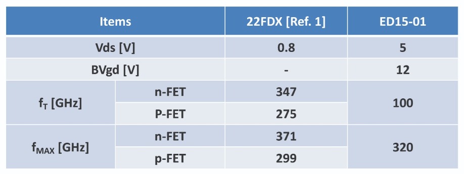
Table 1. Key parameter comparison between 0.15 µm. E-pHEMT (ED15-01) and 22 nm SOI CMOS(22FDX). Data taken from Hoentschel et al., ISTE OpenScience, pp. 6, London, UK, 2019.
Superiority of the DUV stepperThe traditional method for realising a pHEMT with a 0.15 µm gate length or less is electron-beam lithography. However, this technique has a low throughput and a high cost, compromising high volume production.
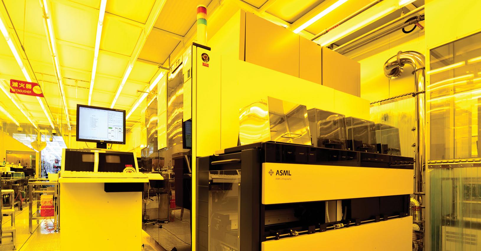
To address these weaknesses, our team at Wavetek Microelectronics Corporation (WTK), a UMC subsidiary, is using the advanced photolithography technology of our parent company. Drawing on this enables us to be the leading commercial GaAs foundry employing a deep-UV stepper. We use this to define 0.15 µm gates in E-mode pHEMTs in a high-volume production environment. This makes our pHEMT technology, produced with a KrF 248 nm stepper, one of a handful of viable candidates for future 5G millimetre-wave MMICs, which must be manufactured using mature, high-volume, low-cost production capabilities.
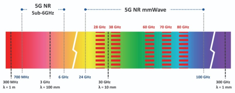
Figure 1. Electromagnetic spectrum for 5G communications
Either MBE or MOCVD can be used to form the heterostructures for pHEMTs, which feature a high-mobility conduction channel created from a two-dimensional electron-gas. On these epiwafers we add drain/source ohmic contacts, formed from an AuGeNi alloy, and a mushroom-shaped Schottky gate, also known as a T-gate (see Figure 2). This gate, created on top of a recess-etched trough, holds the key to forming high-quality, enhancement-mode pHEMTs. The recessed gate region has to be critically etched to ensure a uniform threshold voltage distribution across the wafer, and control wafer-to-wafer reproducibility.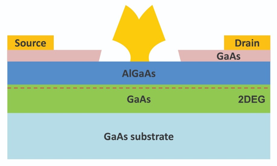
Figure 2. A typical E-mode pHEMT.
We are not the first to turn to stepper technology for the production of compound semiconductor devices. For gates with lengths of 0.25 µm or more, i-line steppers have been used for several decades. But this form of stepper cannot define dimensions of 0.15 µm and below, a domain that is traditionally only associated with direct-write electron-beam lithography. This technique offers flexibility, as it is able to switch between multiple products, but it is limited to smaller volume production.To realize cost-effective, high-volume production of MMICs with a 0.15 µm pHEMT technology within a 6-inch GaAs foundry, we have turned to a deep UV stepper (a typical device, imaged with a scanning electron microscope, is shown in Figure 3). High-volume production commenced in 2018, and at this year’s IMS meeting, we generated significant attention when we unveiled this production ready technology to our peers.
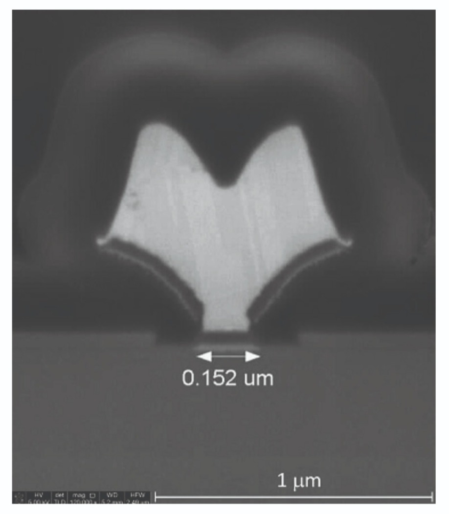
Figure 3. A scanning electron microscopy cross-section image of 0.15 µm gate defined by deep UV stepper photolithography.
A key characteristic of any pHEMT is its threshold voltage. For our enhancement-mode device, it’s about 0.3 V. To determine the degree of uniformity, we have mapped one of our processed wafers with a probe. Results indicate that the standard deviation is just 13 mV (see Figure 4), a value comparable to our 0.25 µm pHEMT technology produced with a standard i-line stepper. The high degree of uniformity highlights the excellent gate threshold voltage controllability of our deep-UV stepper lithography process and our gate-etching process.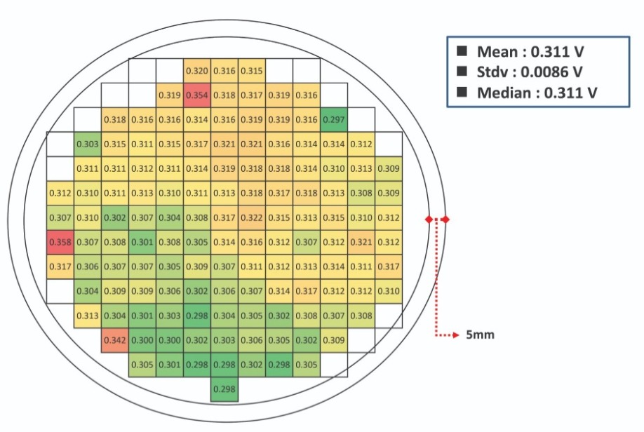
Figure 4. The threshold voltage wafer map of a typical 0.15 µm E-pHEMT device over a 6-inch wafer.
Extensive evaluation To evaluate the yield enhancement provided by our new process, we have used a test vehicle mask to make more than 200,000 discrete, depletion-mode pHEMTs from a 6-inch wafer. A chip probing test reveals the tightly controlled distribution of drain leakage current (see Figure 5).These measurements were made on D-mode pHEMTs, which have a median pinch-off voltage of -0.7 V, at a drain voltage of 4 V and a gate voltage of -1.3 V – that’s 0.6 V deep into the sub-threshold region. The very small variations in the sub-threshold leakage current underscore the tightly controlled threshold voltage. With the new process, wafer yield exceeds 98 percent.
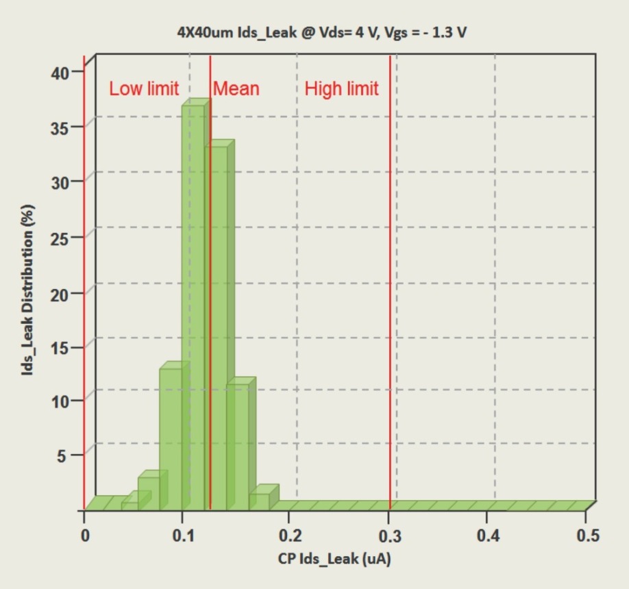
Figure 5. A histogram of a tightly controlled sub-threshold drain current (Ids_Leak) in a 0.15 µm D-pHEMT device used in WTK’s technology development.
Measurements on one of our E-mode pHEMTs with four 75 µm gate fingers reveal that at a gate-source voltage of 0.9 V, the drain-source current is 400 mA/mm, while the maximum extrinsic transconductance is 880 mS/mm at a gate-source voltage of 0.72 V (see Figure 6). Additional investigations show that the drain-to-gate breakdown voltage exceeds 12 V, the typical cut-off frequency is 100 GHz, and the maximum oscillation frequency is more than 300 GHz.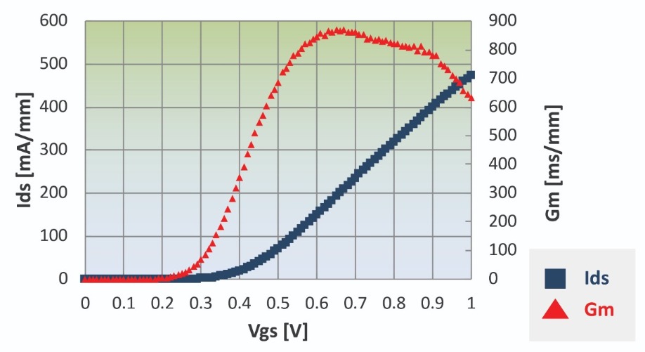
Figure 6. A DC transfer curve of WTK’s 0.15 µm E-pHEMT with gate fingers of a four by 75 µm device.
We have plotted the maximum oscillation frequency as a function of gate voltage at different values of drain bias (see Figure 7). Realising a high maximum oscillation frequency at a high breakdown voltage highlights the great potential of our technology to serve in 5G millimetre-wave communications all the way up to 43 GHz, even with a 5 V power supply.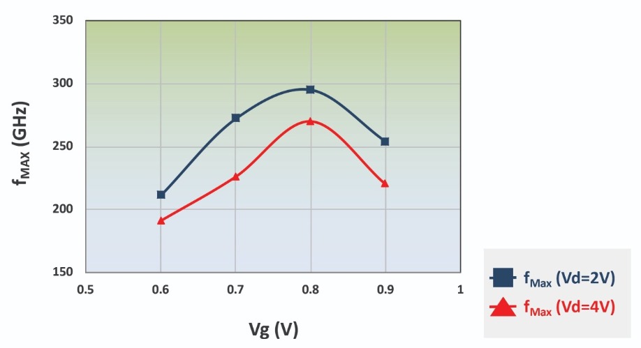
Figure 7. A typical fMAX vs. Vg plot at different Vds of WTK’s 0.15 µm E-pHEMT.
A key requirement for a receiving-end, low-noise-amplifier is a low noise figure. We have conducteda frequency sweep, uncovering the noise figures for an E-mode device with four 75 µm gate fingers. Tests at 12 GHz, under a drain source bias of 3 V and a drain-source current of 10.8 mA, reveal a minimum value for noise of just 0.42 dB and an associated gain of 10.5 dB (see Figure 8). Increasing frequency to 40 GHz produces an increase in noise to 1.27 dB, and trims the associated gain to 5.18 dB. Note that noise is below 1dB at 28 GHz, for a drain-source voltage of 3 V and a current density of 36 mA/mm.
To verify the RF power performance of our 0.15 µm E-mode pHEMT processed with the deep UV stepper, we have designed and produced a one-stage common source power amplifier. It features a transistor with four 75 µm gate fingers to provide the amplification, and several series and shunt transmission lines to match input and output networks. The capacitors are adopted for DC block and bypass networks.
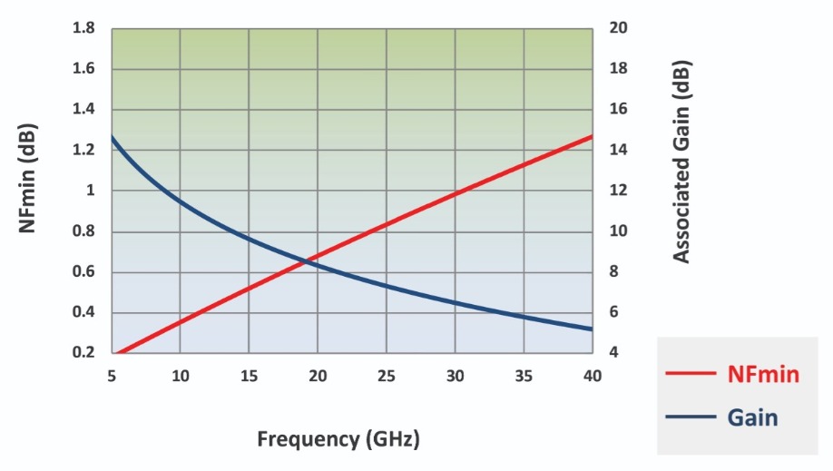
Figure 8. A frequency sweep of noise characteristic of WTK’s 0.15 µm E-pHEMT.
Our power amplifier draws a 60 mA quiescent DC current from a 5 V supply voltage. Power sweeps show that the saturation output power is 22.2 dBm, and the peak power-added-efficiency hits 50 percent at 30 GHz. Power density tops 553 mW/mm, providing further proof that our 0.15 µm technology can provide a good platform for demanding millimetre-wave circuit designs.Today, all 5G millimetre-wave handset PAs are demonstrated in advanced CMOS technology, thanks to its higher integration with CMOS RF front-end and controller circuits in an adaptive array configuration. However, the node required for operation at this frequency has a low breakdown voltage, and a stacking approach involving more than three levels is needed to produce a PA with sufficient output.
Unfortunately, there are downsides to stacking. The effective maximum oscillation frequency tumbles, limiting key high-frequency performance characteristics, such as power density and power-added efficiency. The upshot is a hike in power dissipation and a dramatic decline in power performance, limiting the operating distance of the handset. To address these issues, we advocate a heterogeneous integration approach, combining a CMOS front-end chip with a controller and a high-efficiency, high-power-density pHEMT PA chip. When it comes to selecting the PA, we believe that our 0.15 µm E-mode pHEMT technology is very competitive. Produced with a deep UV stepper, it offers an affordable, high power density, high power-added efficiency solution to address future 5G communications requirements in millimetre-wave bands.
J. Hoentschel et al. ISTE OpenScience, pp. 6, London, UK, 2019
C-M. Chang et al. 2019 International Conference on Compound Semiconductor Manufacturing Technology Digest, pp. 333-336, May 2019.
T. Lodhi et al. Compound Semiconductor IC Symposium, 2006
M. F. O’Keefe et al. IEEE Trans Semicond. Manuf. 16 (2003)
M. M. Abdin et al. 2017 IEEE 18th Wireless and Microwave Technology Conference, 2017


