

Non-contact electrical metrology: trimming costs and slashing time
Widely used in silicon fabs, the corona non-contact C-V technique is now available for wide bandgap semiconductors
BY MARSHALL WILSON FROM SEMILAB SDI
Material AND DEVICE characterisation is an essential step in the production of compound semiconductor devices. To carry this out, foundries and chip manufacturers have dedicated metrology tools that offer a wide variety of characterisation techniques. One of these key techniques is capacitance-voltage (C-V), which provides important information such as dopant concentration, as well as dielectric and interfacial properties.
Standard C-V measurements are well-established, but have significant drawbacks. There is a cost associated with fabricating electrical test structures, and feedback can take weeks. When devices are being developed, this slows progress; and when C-V is used to monitor a manufacturing process, it takes longer for issues to be identified, compromising yield. An additional downside with standard C-V is that it is a destructive test, preventing the use of monitor wafers in subsequent production. To address these issues, the industry needs a non-destructive, cost-effective form of C-V metrology that provides rapid feedback for device development and manufacturing process control.
Fulfilling all of these requirements is advanced corona-based non-contact C-V (CnCV) metrology, developed for comprehensive C-V characterisation of wide bandgap semiconductors, dielectrics and interfaces. It offers a non-destructive, preparation-free alternative to standard C-V that trims manufacturing costs, while slashing the time for data feedback from weeks to just minutes.
CnCV is based on the corona-Kelvin technique that is not new. It is a proven, production-tested method that has been widely adopted in silicon fabs since the 1990s. More than 400 of these tools have been installed worldwide, used primarily for dielectric characterisation. Recently, however, the use of this technique has expanded, so that it can start to serve the wide bandgap power and RF industries through characterisation of SiC, GaN and Ga2O3 based materials.
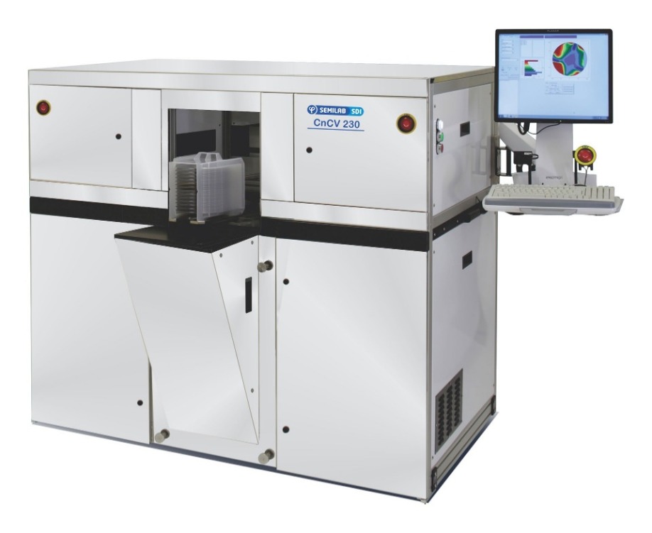
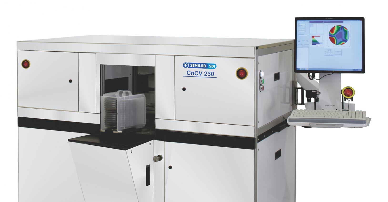
Semilab SDI CnCV 230 tool for non-contact C-V characterisation of wide bandgap semiconductors.
In response to broadening interest from the wide bandgap community, our team at Semilab SDI, based in Tampa, FL, has introduced the CnCV 200 series of tools. Its capabilities include dopant concentration profiling of GaN and SiC, measuring the two-dimensional electron-gas sheet charge in an AlGaN/GaN HEMT, and characterisation of interfaces between dielectrics and wide bandgap semiconductors (for a broader list of capabilities, see Table 1).To control the semiconductor manufacturing process, engineers must map the wafer surface. This enables them to evaluate process uniformity and identify localised defects. Our tool helps them in this endeavour – all of the parameters that are listed in Table 1 can be measured very precisely, at selected locations on a wafer, with results displayed as contour maps that reveal process uniformity.
Principles of CnCV
In CnCV metrology, electric charge that is needed for bias is provided by corona discharge in air. These charges– they may be positive or negative, depending on the selected discharge polarity – are gently deposited on the surface of the wide bandgap semiconductor or dielectric in known charging increments. These charge increments induce a change in surface voltage, which is measured in a non-contact manner, using a vibrating Kelvin probe (see Figure 1). The non-contact capacitance is calculated by dividing the change in charge by the change in voltage. In a corona charge bias sweep, the semiconductor space charge and the surface barrier are cycled between accumulation and depletion. By adopting this approach, the technique provides a full set of data including voltage, charge, capacitance and surface barrier voltage, as well as plots of V-Q, C-Q and C-V. These characteristics form a basis for quantification of the semiconductor, interface and dielectric parameters. Armed with all this information, engineers can gain great insight into the nature of their wide bandgap material and devices.
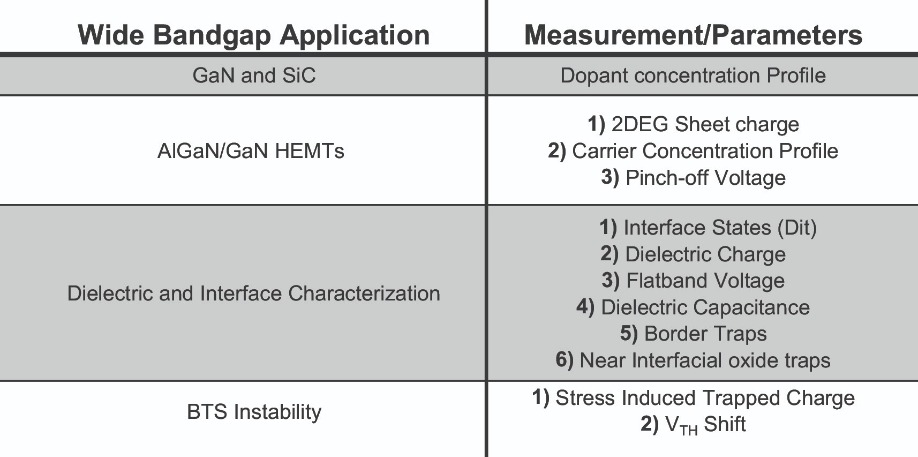
Table 1. Applications of the CnCV technique to wide bandgap materials.
Primary applications for the CnCV technique include dopant concentration measurements and dopant depth profiling. Examples are shown in Figure 2. The CnCV technique offers excellent repeatability and matching to mercury probe for epitaxially grown SiC and GaN (see Figure 3).Characterising promising power devices
One of the wide bandgap power devices that is growing in revenue, and will continue to do so, is the SiC MOSFET. Its attributes include delivering great performance at high fields and high temperatures, but operating in this manner makes the device susceptible to bias- and temperature-induced instability of the threshold voltage. Variations in the threshold voltage stem from complex interfacial instability phenomena, such as near-interfacial oxide trap charging.
To characterise the interfacial properties of dielectrics on wide bandgap semiconductors, engineers now have the CnCV technique at their disposal. It offers a quick assessment of threshold voltage changes before and after bias and thermal stress. This feedback aids investigations of process changes that aim to mitigate this instability, and ultimately improve device reliability.
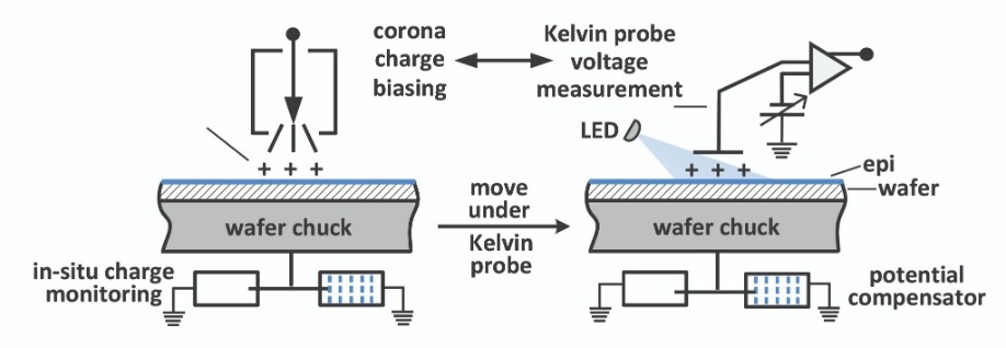
Figure 1. The basic operation of the CnCV technique.
Another promising class of device is that based on the vertical GaN-on-GaN power architecture. High-yield, high-volume manufacture demands the production of many wafers, each with a high degree of uniformity of net dopant concentration. CnCV is ideal for managing this task, because it provides a fast, non-contact, preparation-free method for mapping this characteristic. Note that standard C-V measurements are significantly inferior, as they require costly fabrication of many test structures for full-wafer mapping. To illustrate the capability of CnCV, we have mapped the net dopant concentration for two silicon-doped n-type GaN MOCVD epilayers on GaN substrates (see Figure 4). Comparing the two maps reveals that efforts to improve the growth process were successful, as they reduced the non-uniformity of compensating acceptors.New developments
Recently, there have been several valuable developments in CnCV metrology, enhancing its appeal for the characterisation of wide bandgap semiconductors, dielectrics and interfaces. These new features are focused on characterising aspects of material properties that are critical for wide bandgap device performance and reliability.
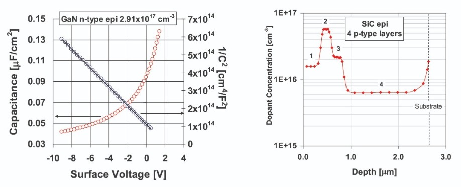
Figure 2. Non-contact corona based CnCV can be used to characterise epitaxial SiC and GaN layers, providing plots of C-V and 1/C2 characteristics (example of n-type GaN on the left). CnCV can also measure dopant profiles on multiple layer epi samples (example of four-layer SiC epi on the right).
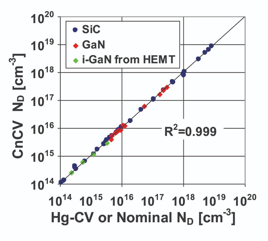
Figure 3. There is a high degree of correlation between CnCV and standard mercury C-V results of dopant measurements on epitaxial SiC, GaN and intrinsic GaN in HEMT structures.
One breakthrough is a unique, direct determination of the flatband voltage. To measure this characteristic, we use a string of photo-induced surface voltage pulses that are generated by low-intensity UV LED excitation of excess carriers. Using this approach, the flatband voltage can be determined without any knowledge of the semiconductor or dielectric properties, or the need to make assumptions regarding the interface state level. That’s not the case for standard MOS C-V, which assumes negligible interface state contribution in the determination of the flatband voltage.It is very valuable to determine an accurate value for the flatband voltage, which serves as an anchor point allowing the determination of the oxide voltage and the surface barrier, at any given charge (see V-Q plot in Figure 5, top). The capacitance-voltage and capacitance-charge (see Figure 5, bottom) characteristics are then calculated.
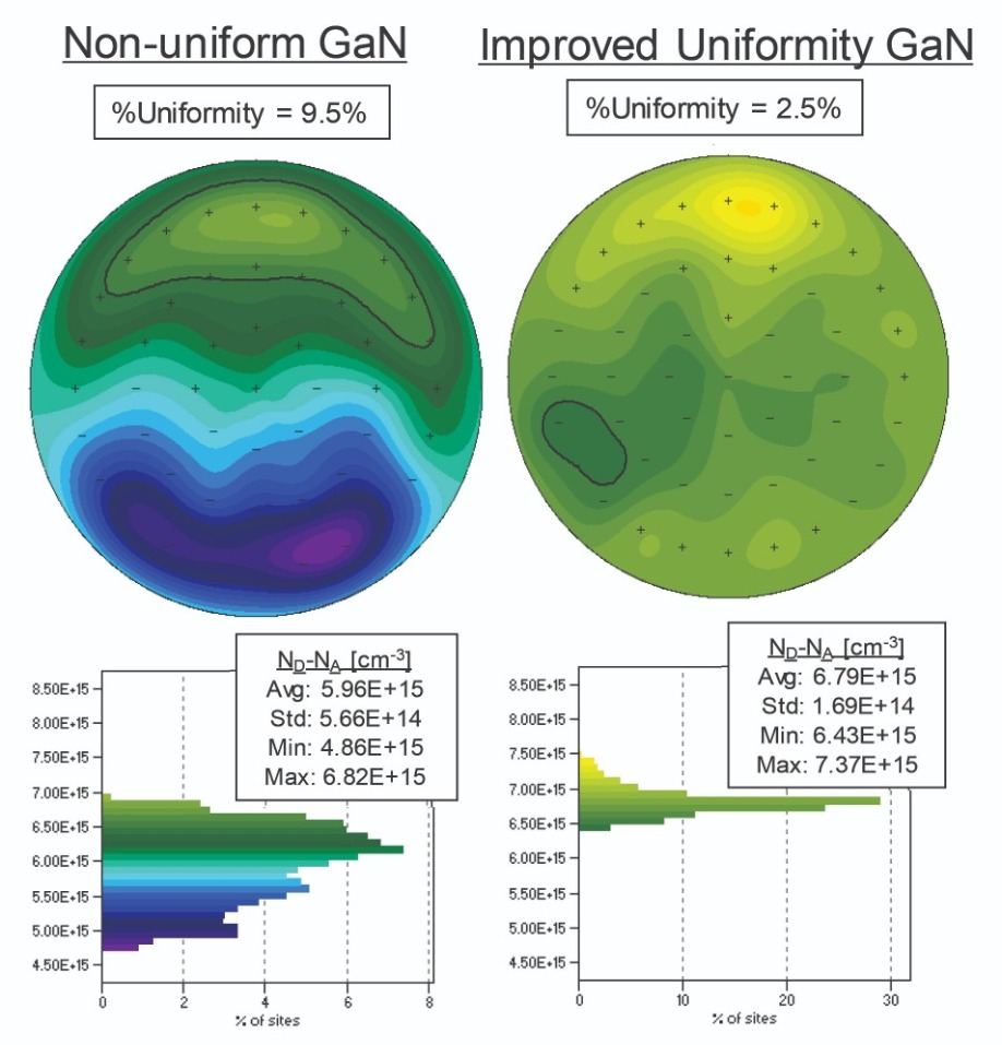
Figure 4. CnCV maps of net dopant concentration on silicon-doped, n-type GaN MOCVD epilayers on GaN substrates show the benefit of process improvement, which reduces the non-uniformity of compensating acceptors.
With knowledge of the surface barrier in the deep depletion condition, the dopant concentration can be determined – and from this, it is possible to calculate the surface charge. Once the surface charge is known, the shallow interface trapped charge density can be obtained directly from the charge neutrality condition.A key feature of materials with a wide bandgap is a large energy separation between the interfacial traps and the edges of conduction and valence bands. Due to this, deep traps cannot maintain occupancy dictated by Fermi statistics, and they remain largely invisible in dark C-V sweeps. Take oxidised n-type SiC, and carry out a sweep that stretches from accumulation to deep depletion, and only shallow interface traps will empty themselves when they move above the Fermi level. Consequently, measurements of interface trap density spectra are limited to about 0.7 eV below the conduction band – that’s less than a quarter of the energy gap. This is a significant impediment, as deep states, uncovered by photo-assisted C-V and current measurements, are known to impact device performance.
To address this concern, we have applied a form of photo-assisted C-V characterisation to our CnCV technique. This addition allows engineers to characterise deep interface states very quickly. We have also adopted the surface photovoltage spectroscopy method, invented back in the 1960s at MIT. This uses a monochromatic source of light with sub-bandgap energy to provide further insight into properties of these deep states.
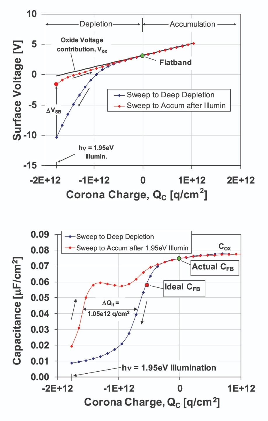
Figure 5. CnCV V-Q (top) and C-Q (bottom) characteristics on n-type SiC with a 45 nm-thick insulating layer of SiO2. Illumination causes photoionisation of interface traps and a negative shift in C-Q characteristic (bottom).
At the heart of our approach are electron photoionisation transitions from interface traps in deep depletion. This process is monitored using a surface voltage transient. With this technique, we have studied oxidized n-type SiC, charged to deep depletion and illuminated with a 635 nm LED that provides excitation at 1.95 eV. Voltage saturation corresponds to empty traps, with this state remaining after turning the light off.We can see the effect of photoionisation in our V-Q and C-Q plots (see Figure 5). Emptying traps decreases the surface barrier, but does not affect the oxide voltage or corona charge. Photons with an energy above the photoionisation threshold depopulate the deep interfacial traps. When the density of trapped interfacial electrons falls, this is manifested as a surface voltage transient (see Figure 6).
With this approach, the magnitude of the change in photoionisation-induced surface voltage gives a measure of the deep interface state concentration. Recording the time constant of the photoionisation decay, using a constant illumination intensity and wavelength, identifies the specific interfacial trap involved in the process – in analogy to the thermal emission constant in deep-level transient spectroscopy.
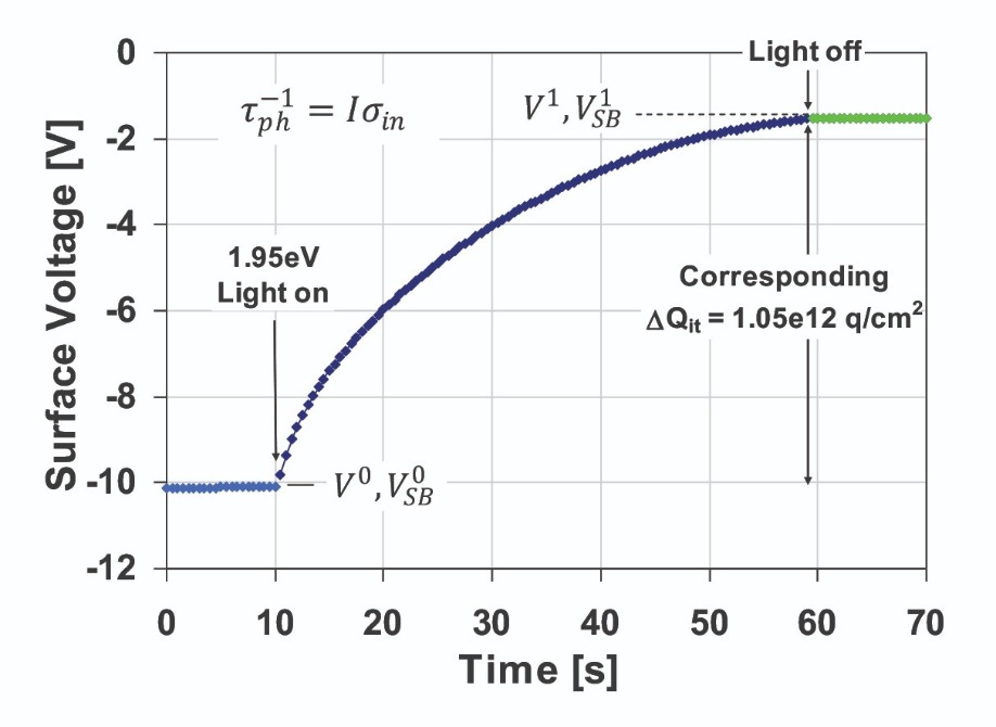
Figure 6. Surface-voltage transients corresponding to Figure 5, resulting from photoionisation of deep interface traps with 1.95 eV illumination.
When deep interfacial traps are emptied by photoionisation, there are changes to the surface barrier height and the semiconductor space-charge capacitance. The latter is associated with the capacitance characteristic measured after illumination. With CnCV, unlike traditional C-V, one can measure a unique capacitance-charge characteristic in addition to a capacitance-voltage characteristic. When there is a change in interfacial charge, it produces a shift of the C-Q curve along the charge axis. For the C-Q results obtained on SiC (see Figure 5), changes to the interface charge are consistent with values obtained from the magnitude of the surface voltage transient (see Figure 6).Illustrating the power of the CnCV technique are measurements made on oxidised SiC, before and after a 850 °C, 8 hour, wet annealing process. Rapid feedback CnCV provides plots of C-Q before and after photoionisation revealing a reduction in deep interfacial states (see Figure 7, top) and shallow interface states (see Figure 7, bottom) by more than a factor of two. This indicates that annealing reduces various types of interface states that are known to cause flatband voltage instability under bias stress conditions. The ability to obtain such quick feedback about the impact of various stages of processing on parameters important for device fabrication can help to greatly improve cost and time savings in process development.
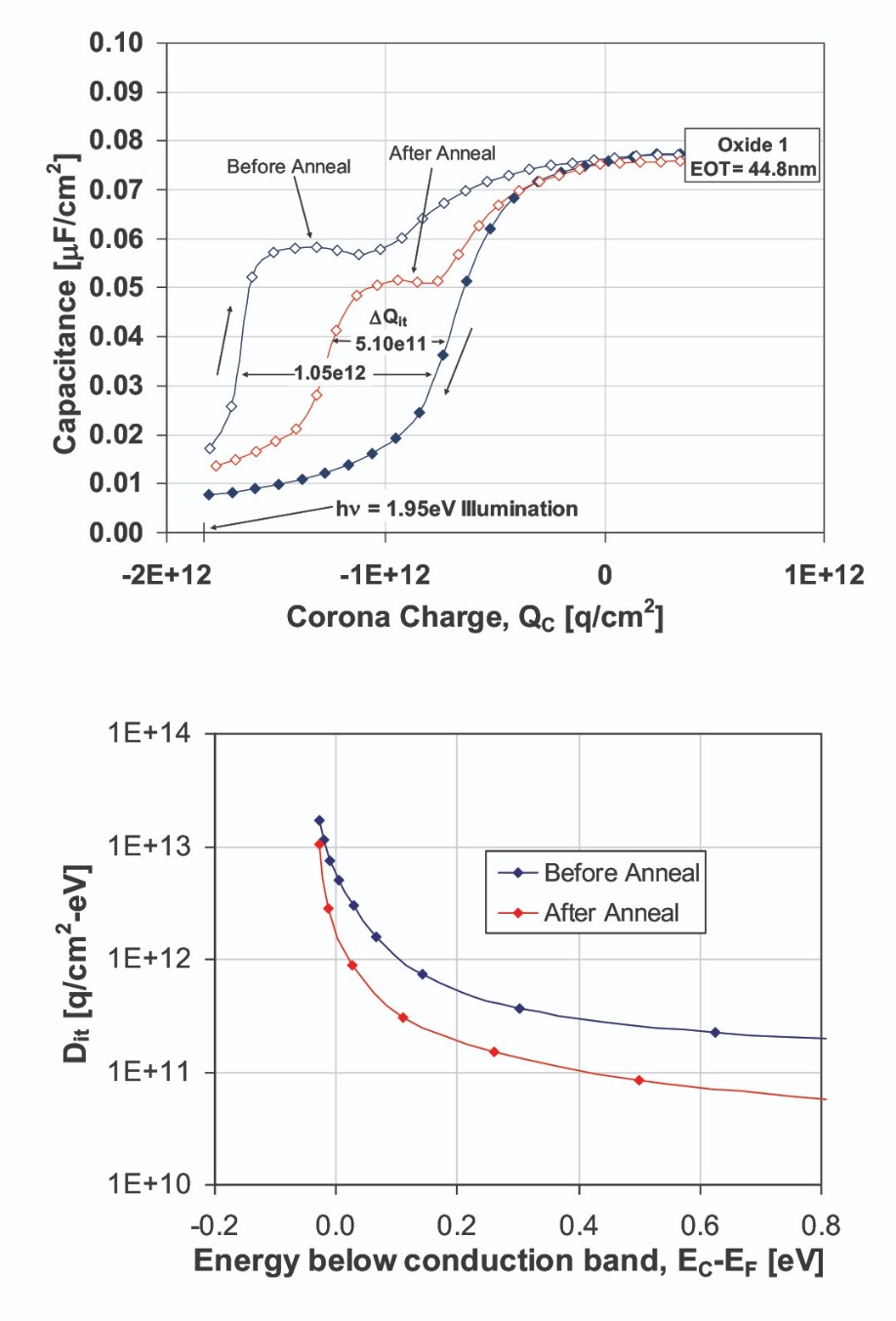
Figure 7. Photoionisation of deep interfacial states using sub-bandgap illumination enables their characterisation using unique photo-assisted CnCV C-Q curves. Example shows reduction in deep (top) and shallow (bottom) interface states before and after a wet post-oxidation anneal.
With sales of wide bandgap power devices rising throughout the next few years and beyond, there will be a growing need for characterising the electrical properties of SiC, GaN and Ga2O3. We have no doubt that the best way to meet this demand is with CnCV, a powerful and convenient non-contact, non-destructive alternative to standard C-V and mercury C-V. CnCV has the upper hand on many fronts: it saves time; it cuts costs; and it offers many unique insights that are not possible with standard C-V, such as direct determination of the flatband voltage and C-Q characteristics. Such attributes will help those that are developing wide bandgap devices, and also those that are ramping production to keep pace with demand.
M. Wilson et al. ECS J. Solid State Sci. Technol. 6 S3129-S3140 (2017)
A. Savtchouk et al. Materials Science Forum 509 858 (2016)


