
VCSELs: Thriving in the heat
Record-breaking modulation speed are realised at elevated temperatures by fabricating VCSELs with two apertures, formed by zinc-diffusion and oxide relief
BY JIN-WEI SHI FROM NATIONAL CENTRAL UNIVERSITY, TAIWAN
Demands on data centres are rocketing. That’s no surprise, given the rise of Netflix, Youtube, social media, and far greater use of the cloud.
To cope with this ever-increasing demand, there have been changes taking place within the infrastructure of the data centre. Historically, coaxial cables have routed data between different central processing units and different mother boards. But these cables are bulky, lossy, and highly dispersive – and they fail to accommodate the tremendous increases in both the data rate and the number of channels in the data centre. So, to overcome this bottleneck associated with the total bandwidth capacity in the data centres, coaxial cables have been replaced with optical fibres. They have the upper hand on many fronts, combining a far lower loss with less dispersion, a broader bandwidth and a smaller form factor. The only downside is that by moving from the electrical to the optical domain for the links, additional electrical-to-optical and optical-to-electrical processes have to be inserted on the transmitting and receiving sides of fibre, respectively.
One option for the light source that generates the data for the optical link is the edge-emitting, distributed feedback (DFB) laser. It is a well-established device, deployed in the traditional optical communication network, where the length of the fibre can be up to thousands of kilometres. The DFB laser dominates this application, because of its high optical output power, low chirp, and a narrow spectral width, a set of attributes that make it ideal for transmitting data over vast distances with very low error rates. But the DFB laser is not a good option in datacentres, where many millions of high-speed light sources have to be densely packaged with ICs, to move data at high speeds between different boards and chips. Its Achilles heel is its relatively high power consumption, which can lead to thermal management issues, wasted heat, and a high carbon footprint for the data centre.
For this particular application, a far better candidate is the VCSEL. In data centres, over 95 percent of fibre channels have linking distances less than 50 metres, so fibre loss and dispersion are not major concerns. In these very-short-reach links, what is paramount is to minimise the electrical-to-optical and the optical-to-electrical conversion losses. And when judged in this manner, the VCSEL wins hands down, consuming just one-tenth of the power of the edge-emitter, thanks to the far smaller size of the optical cavity.
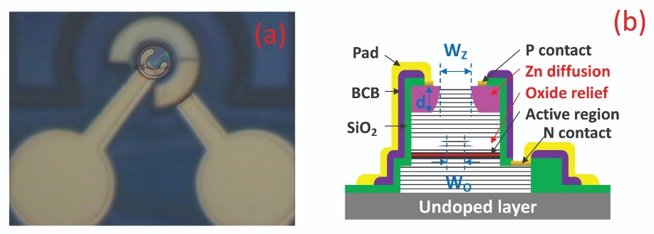
Figure 1. By turning to a double-aperture design, researchers at the National Central University, Taiwan, have set a new benchmark for VCSEL performance. (a) Top-view and (b) conceptual cross-sectional view of the demonstrated device.
VCSELs started to become the dominant source in data communications more than a decade ago. Over the intervening years, a steady stream of improvements to their design have driven increases in the maximum data rates. Ideally, this trend must continue, as it holds the key to a new-generation of data centres that are more frugal that their predecessors. Fail on this front, and the carbon footprint of the data centre could spiral out of control.Working at the National Central University, Taiwan, our team has developed a novel form of VCSEL that sets a new benchmark for performance. This device, a prime candidate for serving tomorrow’s datacentres, features a pair of apertures (see Figure 1). One is defined by zinc diffusion, and allows us to manipulate the number of modes of the VCSEL; and the other is created by oxide relief, and provides us with a lever for the device modulation speed.
A great strength of our device is that it is able to deliver a record-breaking performance at elevated temperatures. For those that build data centres, this is a very valuable attribute. When VCSELs are paired with photodiodes to form transceiver modules, they must be packaged as close as possible to the electronic integrated circuits, which generate a significant amount of heat during high-speed operation. Dense packaging is essential, because it minimises propagation loss and dispersion in the high-speed electrical signals transmitted by the printed circuit board. However, heat generated by the ICs increases the junction temperature of the VCSEL, applying the brakes to the modulation speed.
To serve in the next generation of optical interconnect channels, VCSELs need to have a high-speed performance that is almost invariant with temperature. A data rate of more than 50 Gbit/sec per lane must be maintained between room-temperature and over 85 °C.
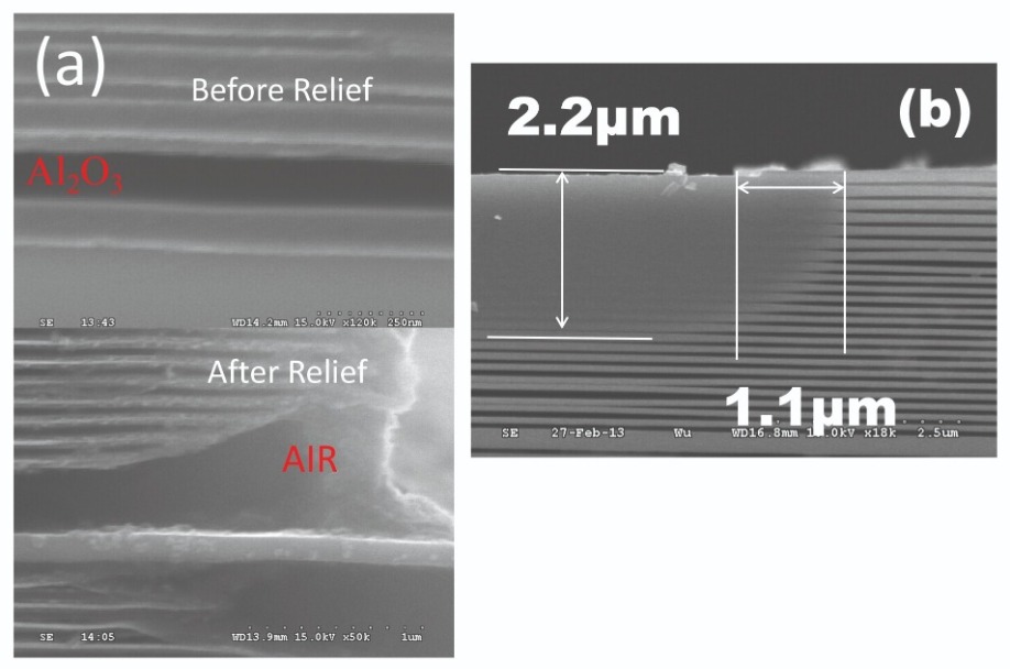
Figure 2. (a) Scanning electron microscopy image of the DBR structure withthe oxide current-confined layer before and after performing an oxide relief process. (b) Scanning electron microscopy image of DBR layers after the zinc-diffusion process.
We have proven that VCSELs based on the GaAs family of materials can meet these requirements. If GaAs-based VCSELs emit at 850 nm, they have an active region that is based on GaAs quantum wells, but if they emit in the spectral range that spans 900 nm to 1000 nm, they have wells made of InGaAs. We work with the latter, because InGaAs wells introduce a larger compressive strain and conduction band offset. These modifications are most welcome, because they minimise the probability of electron leakage under high-temperature operation.Armed with this form of active region, our novel design of 940 nm VCSEL has realised record modulation bandwidths. Judged in terms of optical-to electrical conversion, for a -3dB loss, we have recorded bandwidths of 40 GHz and 32 GHz under room-temperature and at 85 °C. These milestones follow important successes by other groups, such as: a team led by researchers Chalmers University of Technology that reported a 850 nm VCSEL with a 3 dB electrical-to-optical bandwidth of 30 GHz in 2015; and in the same year, a group at the University of Illinois, Urbana Champaign, that announced a multi-electrode VCSEL with a 3 dB bandwidth up to 37 GHz. Recently, the company VI System demonstrated single-mode VCSEL chips with 3 dB bandwidth up to 30 GHz.
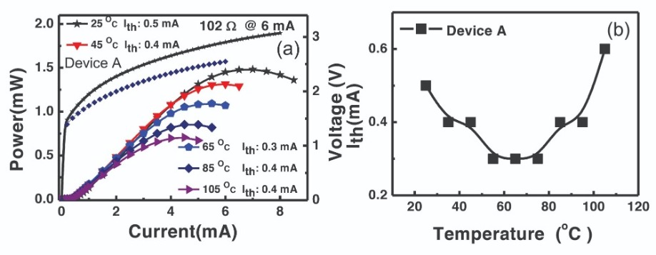
Figure 3.
(a) Measured power-current-voltage curves under different ambient temperatures; (b) corresponding threshold current (Ith) versus ambient temperature.
(b) Figure 4. Bias dependent electrical-optical frequency responses under (a) room-temperature and (b) 85 °C operation. The corresponding bias-dependent output optical spectra under (c) room-temperature and (d) 85 °C operation.
(c) Figure 5. The measured (a) 50 Gbit/s at room temperature, (b) 50 Gbit/s at 85 °C, and (c) 60 Gbit/s at room temperature OOK transmission eye-patterns over 1 m OM5 fibre (back-to-back) without signal processing; (d) corresponding bathtub curves. The bias current and peak-to-peak driving voltage (Vpp) applied to the device during measurement are 5 mA and 0.55 Vpp, respectively
We fabricate our VCSELs by processing epiwafers purchased from Landmark. Grown on an semi-insulating GaAs substrate, our epiwafers feature: an active region with several InGaAs quantum wells; an aluminium-rich AlGaAs oxidation layer that sits just above the active region; and a pair AlGaAs-based distributed Bragg reflectors, which form the mirrors either side of the active region (see Figure 1).
Our first step is to process these epiwafers into mesa structures with diameters of typically 30 µm. After this, we employ wet oxidation and oxide-relief processes to selectively remove the AlxO1-x current confined layer. During these two processes, oxidation takes place in the oxide current-confined layer and also at the edge of distributed Bragg reflector layers with high aluminium concentrations. Consequently, both are subsequently etched away (see Figure 2 (a), which shows scanning electron microscopy images of our oxide aperture before and after the oxide relief process).
The oxide-relief process is beneficial. As the refractive index of air is much smaller than that of the AlxO1-x layer – it is 1, rather than 1.6 – there is a further reduction in the parasitic capacitance of the oxide-relief device. This leads to an increase in the bandwidth of the VCSEL, so that it can operate at a higher data-rate.
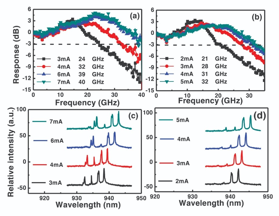
Figure 4. Bias dependent electrical-optical frequency responses under (a) room-temperature and (b) 85 °C operation. The corresponding bias-dependent output optical spectra under (c) room-temperature and (d) 85 °C operation.
In a typical VCSEL, there is just one aperture, formed by oxidation. But in our devices, we have a second one, created by zinc-diffusion. A downside of the diffusion process is that it supresses the local lasing phenomenon: threshold gain increases in the zinc-diffused region, due to a rise in free-carrier absorption loss; and there is also a reduction in reflectivity. However, there is an upside too, as zinc diffusion enables mode control, a key to improving the quality of data transmission through an optical fibre. Improving mode control trims chromatic dispersion, and in turn increases the transmission distance, which can be valuable in modern data centres that have expanded to several buildings to accommodate the demand for more data, and may contain links of a kilometre or more.
We use a high-quality Si3N4 layer to create a diffusion mask that controls the location of the zinc within our device. Inspecting the distributed Bragg reflector after the diffusion process shows that it introduces a great deal of disorder – the individual layers are no longer visible with a scanning electron microscope (see Figure 2 (b)). This disordering is beneficial, as it reduces the contact resistance when the injected current flows through the distributed Bragg reflector.
To evaluate the performance of our VCSELs, we have plotted their current-voltage-light characteristics and their threshold current over temperatures ranging from ambient to 105 °C (see Figure 3). These measurements show that over that temperature range the increase in the threshold current is very small – it is less than 0.2 mA. We attribute this to the large conduction band offset in the AlGaAs/InGaAs active region, which minimizes electron leakage.
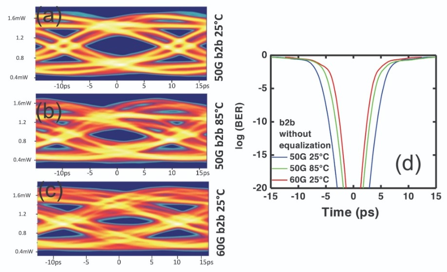
Figure 5. The measured (a) 50 Gbit/s at room temperature, (b) 50 Gbit/s at 85 °C, and (c) 60 Gbit/s at room temperature OOK transmission eye-patterns over 1 m OM5 fibre (back-to-back) without signal processing; (d) corresponding bathtub curves. The bias current and peak-to-peak driving voltage (Vpp) applied to the device during measurement are 5 mA and 0.55 Vpp, respectively
Another attribute of our VCSELs, highlighted in Figure 3, is their low differential resistance. Under a 6 mA bias current, differential resistance is as low as 100 Ω at room temperature, and just 80 Ω at 85 °C. In comparison, conventional 980 nm VCSELs with a similar size of oxide aperture – that is, about 3 mm – have differential resistances of typically 200 Ω at 85 °C. The superiority of our devices stems from the zinc-diffusion process and the topmost current-spreading layers.
We have also measured the bias-dependent electrical-optical frequency responses of our VCSELs, and their corresponding output optical spectra, at both room temperature and 85 °C (see Figure 4). The graphs show that the maximum 3 dB electrical-optical bandwidth can hit 40 GHz at room-temperature, and is still as high as 32 GHz at 85 °C.
Additional measurements have been made to evaluate the capability of our VCSELs to transmit data through a fibre. They include 50 Gbit/s and 60 Gbit/s on-off keying transmission results with eye-patterns and corresponding bathtub curves for the device under room-temperature and 85 °C operation over a 1 m OM5 fibre (see Figures 5 (a) to (d)). These results are very encouraging. At 50 Gbit/s, the bit-error rate is below 1 x 10-12, all the way from room-temperature up to 85 °C, without any pre-emphasis or equalisation techniques. In other words, over this temperature range, we have produced bit-error-free transmission. What’s more, at room temperature, the maximum error-free data rate can be as high as 60 Gbit/s.
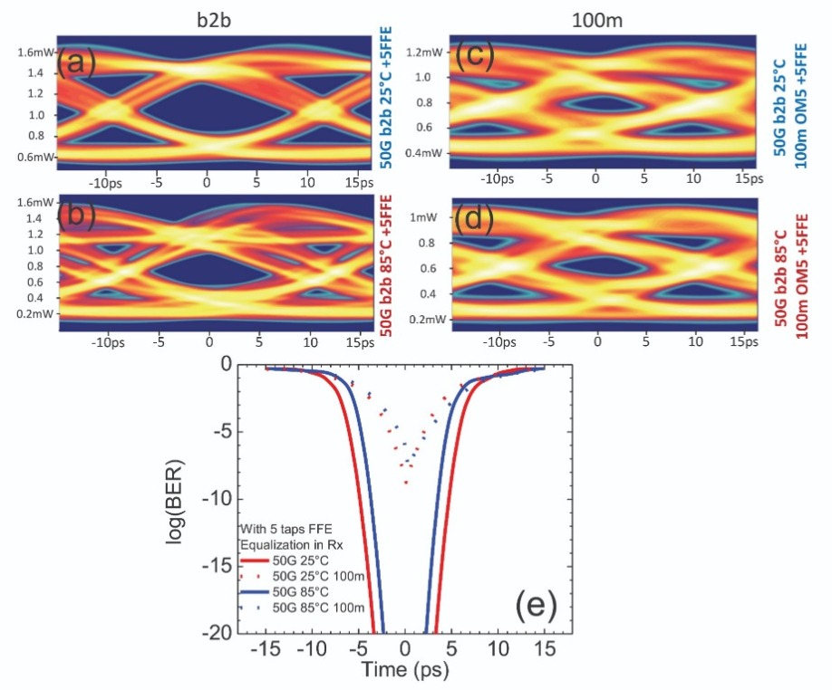
Figure 6. (a) 50 Gbit/s eye patterns measured at 25 °C and back-to-back transmission; (b) 50 Gbit/s eye patterns measured at 85 °C with back-to-back transmission; (c) 50 Gbit/s eye patterns measured at 25 °C and 100 m OM5 fiber transmission; (d) 50 Gbit/s eye patterns measured at 85 °C and 100 m OM5 fibre transmission with FFE equalization; (e) corresponding bathtub curves.
We have also investigated transmission over 100 m, using the same type of fibre (see Figure 6). In this case, standard five taps feed-forward equalisation is used at the receiver end to compensate for the limited bandwidth of around 32 GHz. Results show that we can realise invariant 50 Gbit/s transmission performance, with a bit error rate below 1 x10⁻⁷, from room temperature to 85 °C.Our results are very encouraging for the future of very-short-reach optical interconnect networks. The capability of these novel VCSELs over a wide temperature range makes them very attractive candidates for data centres. In addition, they could also serve in other harsh environments. They could, for example, deliver data transmission inside autonomous cars and drones, opening up yet more markets for what is arguably the most exciting compound semiconductor device of our age.
J.W. Goodman et al. Proc. IEEE. 72 850 (1984)
D. M. Kuchta et al. IEEE Photon. Technol. Lett. 27 577 (2015)
E. Haglund et al. Electron. Lett. 51 1096 (2015)
S. T. M. Fryslie et al. IEEE Photon. Technol. Lett. 27 415 (2015)
G. Larisch et al. IEEE Photon. Technol. Lett. 28 2327 (2016)
Jin-Wei Shi et al. IEEE J. of Sel. Topics in Quantum Electronics 19 7900208 (2013)
Chen-Lung Cheng et al. Proc. OFC 2019, San Diego, CA, USA, March, 2019, W3A.2.


