
Amplifying ammonothermal growth

Near-equilibrium ammonothermal growth of multiple GaN crystals in a single vessel realises high throughout and great material quality
By Tadao Hashimoto FROM SixPoint Materials
The success of the Blu-ray player has worked wonders for our industry. It has not only given the GaN laser and its native substrate their first killer application – it has been instrumental in driving improvements in material quality. Makers of BluRay players strive for reliable products, and thus reliable lasers, so to achieve that there has been much effort directed at reducing the dislocations in the underlying GaN substrate. If it doesn’t meet the mark, it is LED-grade rather than laser-grade, and can only be used for the production of ultra-high brightness LEDs.
Twenty years on from the first commercialization of free-standing GaN wafers by HVPE, this market is now worth many tens of millions of dollars (according to market analyst Yole Développement, sales totalled $60 million in 2017). But it could be worth even more, if GaN substrates can set a new benchmark for material quality. Exceed on that front and they can underpin the development of high-power electronic and optoelectronic devices.
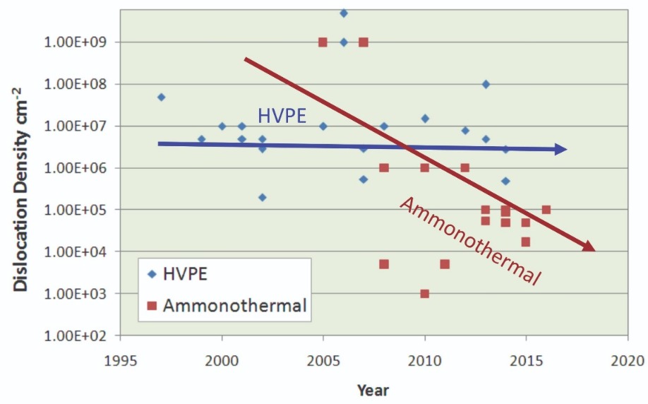
Figure 1. Historical trend of dislocation reduction in GaN.
Efforts at developing GaN-based devices with a high power-handling capability include a number of projects supported by the Advanced Research Projects Agency – Energy (ARPA-E), a division within the US Department of Energy (DoE). Back in 2014, ARPA-E launched the SWITCHES programme, aimed at developing 1200 V, 100 A power devices. Research focused on devices with a GaN-on-GaN vertical architecture. Following on from this, several projects supported by ARPA-E kicked off this March, targeting 15-20 kV GaN-on-GaN devices and systems. In the US, further backing of this technology is coming from the Office of Naval Research of the US Department of Defense (DoD) – it is conducting a 20 kV GaN-on-GaN device programme. In addition, there are similar programmes underway in Japan.All these efforts have been motivated by the need for high-power, high-efficiency electronic devices. More and more engineers are recognising that the best way to realise them is through a GaN-on-GaN architecture. Devices will need to combine an incredibly low leakage current in extreme reverse bias with the capability to handle a great deal of heat, to ensure reliability. Crucial to meeting these two goals are GaN substrates with a lower dislocation density than today’s laser-grade material.
Such a platform is also an essential ingredient in the production of multi-mode, high-power blue lasers. If they produce an output of 100 W or more, they can be used for machining. To produce such a source, engineers are trying to draw as much power as possible from each device within a laser array. Success hinges on handling a great deal of thermal, electrical and optical energy. For these extreme power lasers, the GaN substrates that provide their foundation must have a dislocation density that is below that found in today’s laser-grade material.
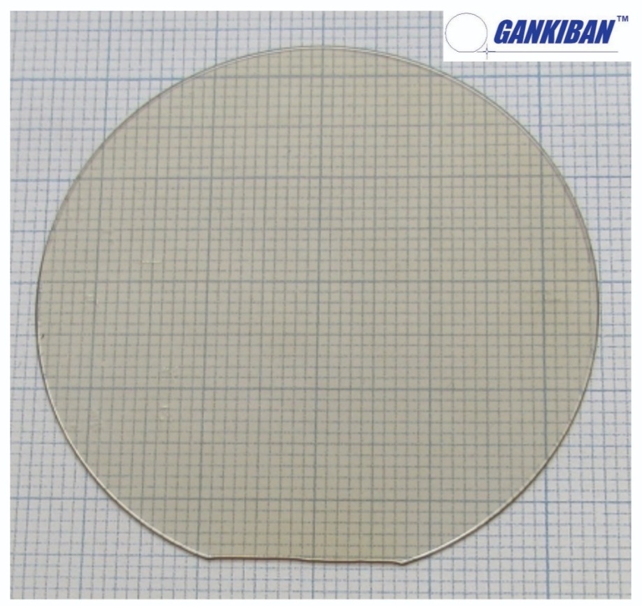
Figure 2. Near-equilibrium ammonothermal growth has been used to produced 2-inch GaN substrates.
Obstacles to successThere are two significant hurdles that must be overcome in order to enable the production of ‘power-grade’ GaN substrates with sufficient quality for the manufacture of high-power electronic devices and lasers. One is an improvement in quality, driven by a reduction in dislocation density. Progress with HVPE-grown material has stagnated over the last 15 years, with dislocation densities typically in the low-to-mid-106 cm-2; and the chances for a breakthrough are not great. Progress is held back by a lack of understanding of how to reduce defects in thick layers – those that are 100 µm or more – and the mechanism behind the generation of these imperfections. Plot the reduction in dislocations over time (see Figure 1), and results suggest that it is unlikely that there will be a significant reduction in the dislocation density in HVPE-grown material. However, there is hope, as the ammonothermal method is yielding better and better material, and further improvements are promised.
The second obstacle to power-grade material is market deadlock. Customers want more substrates at a lower price, but manufacturers can’t increase production volume without pushing up the price. Although the price of a 2-inch GaN substrate has dramatically declined over two decades, thanks to intensive, patient improvement of the HVPE process,
it appears that it cannot go any lower. Today, the leading manufacturers of GaN substrates are producing their material with fully depreciated HVPE equipment. To increase production, they would need to invest in new equipment, and recoup this outlay through an increase in the price of the substrate. So far, the producers of HVPE GaN substrates have not ventured down this road, despite increasing market demand.
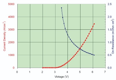
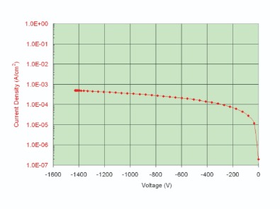
Figure 3. Current-voltage characteristics for p-i-n diodes fabricated on GaN substrates produced by near-equilibrium ammonothermal growth. Device growth, fabrication and characterization were conducted by R. Dupuis, S-C. Shen and T. Detchprohm at Georgia Tech.
Breaking throughAt SixPoint Materials of Buellton, CA, we can overcome both of these obstacle with our near-equilibrium ammonothermal (NEAT) technology. In general, material made with ammonothermal approaches is decreasing in dislocation density year on year. For us, the typical density of our latest 2-inch substrate is low-to-mid-105 cm-2. Lower figures should follow, making our product an attractive candidate for makers of next-generation, high-power electronic and optoelectronic devices that are in search of power-grade GaN substrates.
Similar to the hydrothermal method used for the mass production of quartz, the ammonothermal technique uses supercritical fluid, which has a low viscosity and a high circulation speed. These characteristics enable a uniform temperature inside the reactor, which is a great attribute, as any non-uniformity of temperature on the growth front hampers scaling.
The ammonothermal method is renowned for its low growth rate. It typically takes an entire day to grow 100 µm, while HVPE could realise this is just an hour. Given this substantial difference, it’s no surprise that many groups have focused on increasing the speed of their ammonothermal process. Typically, this is realised by increasing the driving force of crystal growth. However, that has a downside: it results in unwanted heterogeneous nucleation inside the reactor. Once GaN nucleates, it consumes the source, leading to a drop in growth rate. Such conditions impair consistent crystal growth and deteriorate the quality of the material.
We take a different tack, growing many crystals simultaneously in a large reactor, with the growth condition near equilibrium. Using this approach, we minimise parasitic deposition, and as the crystals grow thicker, their quality improves. Although the growth rate is slow, by growing many crystals simultaneously, we compensate for this.
Thanks to the strong support of ARPA-E and DoE, we have made great progress in the development of our 2-inch GaN substrates. We refer to them as Gankiban. In Japanese, this is literally ‘GaN substrate’.
Through an intensive study of crack generation during our growth of bulk GaN, we have been able to identify the key culprits of crack generation. This insight enables us to produce 2-inch crack-free substrates (see Figure 2). They have an excellent microstructure, according to X-ray diffraction rocking curves, which have an average full-width at half-maximum of 20-70 arcsec. The dislocation density of this material, determined by defect-selective etching, is low-to-mid-105 cm-2.
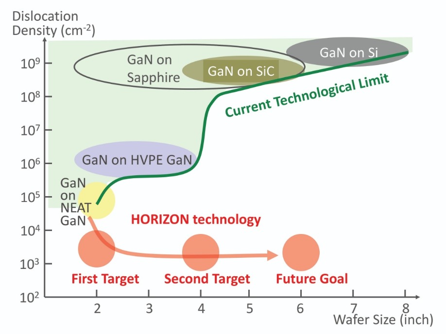
Figure 4. Current GaN technology mapped in terms of wafer size and dislocation density. HORIZON technology aims to address this dilemma and achieve low-dislocation, large-area GaN substrates.
Another attribute of our substrates is that they have less bow than those made by HVPE. Curvature is typically in the range of 10 m to 40 m. A low curvature is highly valued, because it determines the uniformity of the miscut angle. Variations in the miscut angle are detrimental, degrading the surface morphology of thick drift layers used in power electronic devices, and broadening the emission wavelength of the InGaN active layer in LEDs and lasers.Through our funding from the DoE, as well as optimising our ammonothermal growth process, we have been able to develop a technology for forming high-quality substrates from our crystals. Establishing a back-end wafering process is just as important as having one for crystal growth, because it is needed to make the power-grade substrates that are the bedrock for the production of high-quality epitaxial films.
We can offer this to our customers – our Gankiban substrates are epi-ready on the gallium face, and have miscut angles of 0.4°±0.1° along the m-direction and 0.0°±0.1° along the a-direction. These attributes enable the growth of high-quality GaN layers with thicknesses of 10 µm or more that will lie at the heart of high-power diodes and transistors.
Working within the ARPA-E SWITCHES program, our collaborators have used our substrates to make and then characterise p-n diodes, p-i-n diodes, and high-power diodes. Researchers at Georgia Tech have measured forward and reverse current-voltage characteristics of p-i-n diodes that have a drift layer consisting of 4 µm of lightly doped n-type GaN and 6 µm of undoped GaN (see Figure 3). Characterisation reveals a reasonable on-resistance and a breakdown voltage of over 1400 V.
Other teams that used our substrates to make high-power diodes have also enjoyed success. This shows that our substrates have a high degree of compatibility with various kinds of MOCVD reactors, and that they are well suited for power device applications.
Future prospects
Our successful demonstration of a 2-inch GaN substrate has paved the way for pilot production. We are currently raising $5 million to increase the number of production reactors. Our method for producing GaN and our associated technologies are well protected – we have over 100 patents world-wide, and there are about an additional 40 patents pending.
Efforts at developing our technology are focusing on four areas: clear Gankiban, insulating Gankiban, further reductions in dislocation density, and an expansion in the size of our substrates. Today, the substrates that we ship are slightly coloured, due to a high concentration of oxygen in the crystal (see Figure 2). Our material has an oxygen concentration of about 2 x 1019 cm-3, making it heavily n-type. This high electrical conductivity is beneficial for vertical power electronic devices and laser diodes, but its coloration is not acceptable for LED applications, and also not for some VCSEL applications. Another drawback of the high concentration of oxygen is that it could have an adverse effect on the thermal conductivity of the wafer.
Through process purification and optimization, we have recently been able to reduce the oxygen concentration in our material to 2 x 1018 cm-3. This yields transparent, clear Gankiban. We plan to release this form of GaN substrate in late 2019. It will contribute to further implementation of GaN-on-GaN LEDs, and offers added values of a low lattice bowing and low-cost production.
We are developing insulating Gankiban for RF applications, because this could be a superior alternative to SiC. Using GaN rather than SiC as the substrate for the GaN RF HEMT will reduce thermal conductivity, but this drawback could be overshadowed by the reduction in defects in the device layer that might limiting the performance of the device. What’s more, the buffer layer that is required for epitaxial growth of GaN on SiC might be a thermal barrier, eradicating the benefit of the high thermal conductivity of SiC.
The other two goals that are high on our agenda are to reduce the dislocation density of our substrates and increase their size. Compared with other compound semiconductors, GaN has a long way to go. Even the best material, GaN made with our ammonothermal technique, has a relatively high dislocation density – and this, and HVPE-grown GaN, are limited in substrate size. Going to GaN-on-silicon addresses the size issue, but the price to pay is a hike in the dislocation density. We are trying to tackle both of these issues head-on by developing 6-inch GaN substrates with a dislocation density of just 103 cm-2 (see Figure 4 for our roadmap).
This effort will build on our development of our 2-inch power-grade GaN substrates that will provide a great foundation for the next generation of high-power electronic and optoelectronic devices. They address the two key requirements of these chipmakers – a low-dislocation density and a more competitive price.
The work introduced in this article has been conducted under the support of the ARPA-E SWITCHES program (DE-AR0000445) and the DoE EERE AMO SBIR program (DE-SC0013791). p-i-n diodes were grown, fabricated, and characterized by the research group of Prof. Dupuis, Prof. Shen, and Dr. Detchprohm at Georgia Tech.


