
Nanocrystals light up ultraviolet optoelectronics
AlGaN nanocrystals have great potential for raising the performance of UV LEDs and laser diodes, thanks to their negligible defects and dislocations, highly efficient p-type conduction, and efficient light extraction
BY XIANHE LIU AND ZETIAN MI FROM THE UNIVERSITY OF MICHIGAN
UV light emitters serve a broad range of applications. They can be used to provide purification of water and air; deliver disinfection, curing, bioagent analysis and detection; and provide the light source for fluorescence spectroscopy. But all of today’s common UV sources are far from ideal. Whether it is a mercury lamp, an excimer laser, or a diode-pumped solid-state laser that produces UV emission, the source suffers from a large footprint, a low energy efficiency and a limited emission wavelength, and it uses toxic material. What’s more, when viewed from an environmental perspective, all these forms of UV emitter are unsustainable.
Far more promising alternatives are LEDs and laser diodes. These sources, which reach the UV with AlGaN alloys, are far smaller, safe in operation, and able to target a specific wavelength. This expands the number of applications that the UV source can serve.
However, before UV LEDs and lasers can become considerable commercial successes, a few challenges have to be overcome. High on this list is the limited spectral range – to date, the shortest reported wavelength for an electrically injected AlGaN quantum-well laser is 336 nm. Another drawback of this device is its large threshold current density, which is on the order of at least 10 kA cm-2. Like the laser, the performance of the LED is vastly inferior to the visible cousins, with an efficiency well below 10 percent in a large part of the UV-C spectrum, which spans 100 nm to 280 nm. The losses come from inefficient light extraction, the presence of a large density of defects, and poor p-type current conduction.
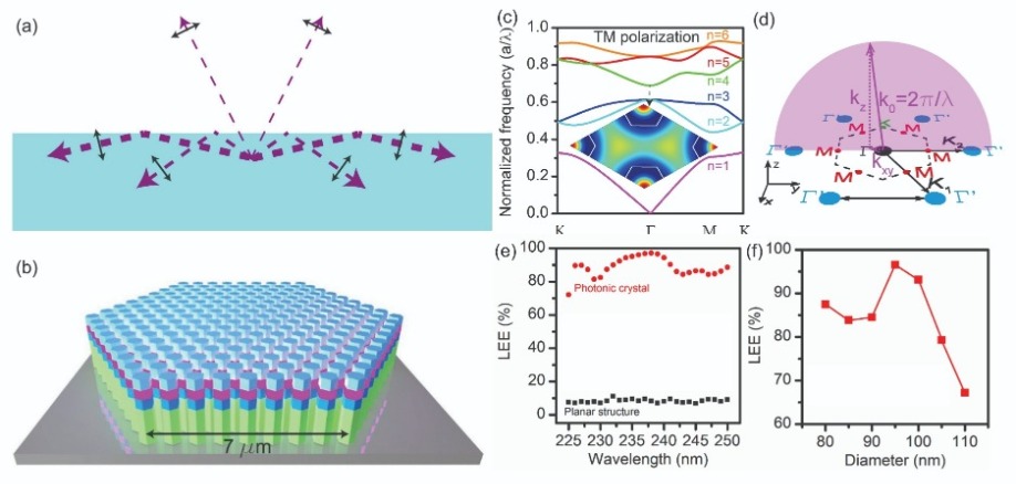
Figure 1. (a) Planar structures are impaired by a poor light extraction efficiency due to total internal reflection. (b) The light extraction efficiency is higher for a photonic crystal structure. (c) Photonic band structures are calculated for a lattice constant of 160 nm and a diameter of 95 nm. The electrical field intensity profile for the Γ point at the band n=4 indicates that there is a large overlap between the centre of nanocrystals and the maxima of the electric field intensity profile. This aids the output power of a nanocrystal LED. (d) Light with a wavelength of 240 nm has zero wavevector (Γ point at the band n=4). With a wavevector that is either zero or negligible in the horizontal plane, light emission is primarily coupled into the vertical direction. (e) Light extraction efficiencies calculated for a photonic crystal structure and a planar structure. (f) Variation in the light extraction efficiency with diameter. For more details, see X. Liu et al. IEEE Photon. J. 10 1 (2018).
It is widely accepted that the poor performance of UV lasers and LEDs stems from the conventional growth techniques for the AlGaN alloy and the basic material properties. To overcome these bottlenecks, there needs to be new approaches to growing the material and engineering the material properties.At the University of Michigan we are trying to succeed on these fronts with arrays of AlGaN nanocrystals. This approach has much promise. One of its merits is that it is possible to realise a light extraction efficiency in excess of 90 percent by arranging nanocrystals in a photonic crystal structure, a geometry that is compatible with large-area LEDs. Taking this approach, we have produced devices spanning 210 nm to 360 nm that have efficient p-type doping, one of the issues in conventional devices. What’s more, we have made a low-threshold, electrically pumped nanocrystal laser operating at 369.5 nm, by engineering the optical properties via the photonic crystal structure.
Efficient light extraction
Mid and deep UV LEDs have an extremely low efficiency, due to the dominance of transverse-magnetic-polarized optical emission. In these devices, the electric field of the emitted light is parallel to the c-axis, due to the negative crystal-field splitting energy in aluminium-rich AlGaN. One consequence of this is that the majority of light is emitted out of the active region in the horizontal direction (see Figure 1 (a)), and it cannot be extracted out of the chip due to total internal reflection. The resulting light reabsorption inside the device is highly detrimental, leading not only to an extremely low efficiency, but also causing severe heating and device instability.
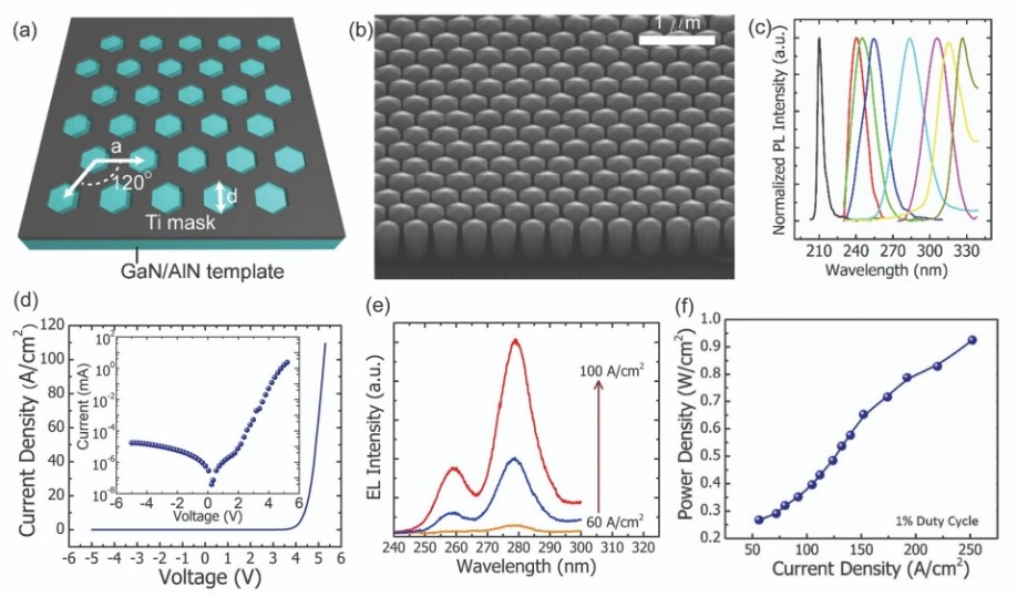
Figure 2. (a) Nanocrystal structures are produced by first patterning a growth mask on the substrate. (b) A scanning electron microscopy image of AlGaN nanocrystals formed by selective-area epitaxy. (c) Photoluminescence spectra of AlGaN nanocrystals with an aluminium-content varying from 20 percent to 100 percent. (d) Current-voltage characteristics of an LED based on AlGaN nanocrystals formed by selective-area epitaxy. Inset: Current-voltage characteristics plotted on a semi-log scale. (e) Electroluminescence spectra under varying injection current density. (f) Variation of output power with injection current density, measured using a pulsed biasing condition. For more details, see: X. Liu et al. Opt. Express 25 30494 (2017)
To see if we can address these issues, we have undertaken finite-difference-time-domain simulations to investigate whether photonic nanocrystals can improve light extraction. These simulations consider emission at 240 nm, for nanocrystals that have a lateral size of 95 nm and are spaced apart by 160 nm (see Figure 1 (b)). By calculating the relation between the wavelength and the wavevector in these photonic crystals, we have determined that light emission is primarily coupled in the vertical direction (see Figure 1 (d)). Another encouraging aspect of this design is that there is a large overlap between the centre of nanocrystals and the maxima of the electric field intensity profile. This aids the output power of the nanocrystal LED.The benefits of the nanocrystals are so substantial that they can clear the bottleneck of light extraction, which has been hampering efforts to improve deep UV LEDs for many years. While extraction efficiency for planar structures is below 10 percent, in photonic crystals it can exceed 90 percent.
Note that the photonic crystal structures that we are investigating are not just designs for hero results in a lab. The architecture is robust, offering reasonable tolerance for deviations in dimensions. Even if the 95 nm target is missed and diameters vary from 80 nm to 100 nm, the efficiency of light extraction is still around 85 percent or more, implying that this device has much commercial promise.
Selective area epitaxy
The majority of III-nitride nanostructures are grown on foreign substrates through a self-organisation process. However, that is no good to us, as it creates nanocrystals with random diameters at random positions. Instead, we employ selective-area epitaxy to achieve site-controlled growth of nanocrystals with a well-defined size and position. This involves using a growth mask to promote the growth of nanocrystals on the template, in favour of growth in the apertures on the mask.
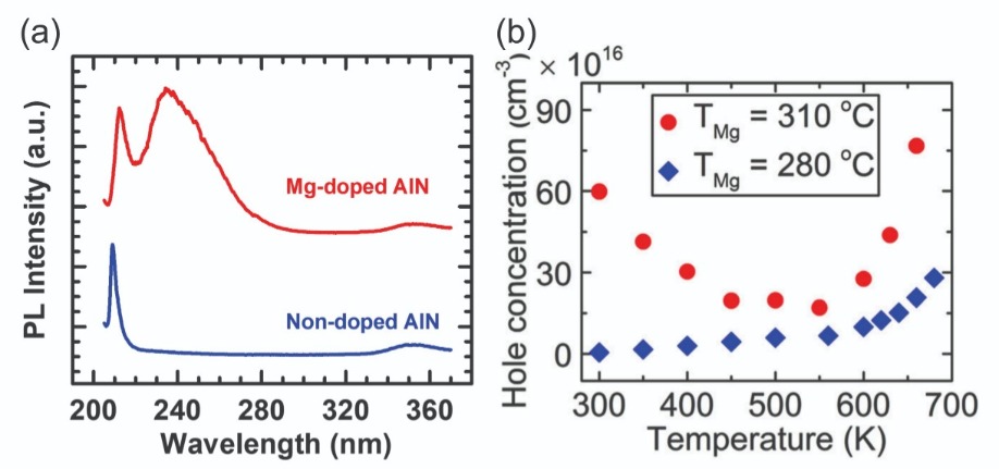
Figure 3. (a) Photoluminescence spectra for magnesium-doped AlN and non-doped AlN nanocrystals. (b) Variation of hole concentration with temperature for samples with two different magnesium doping levels (different magnesium cell temperatures). For more details, see; X. Liu et al. Photonics Res. 7 B12 (2019); and N. H. Tran et al. Appl. Phys. Lett. 110 032102 (2017)
To produce our nanostructures, we take a GaN (or AlN) template formed on sapphire, and deposit a thin titanium mask on top. This is followed by electron-beam lithography and dry etching, to create nanoscale aperture arrays (see Figure 2(a)). Then, through the use of optimised growth conditions, we ensure epitaxy takes place in just the apertures, to create nanocrystals with a precisely controlled size and spacing (see Figure 2(b)). With this approach, we can produce AlGaN nanocrystals with an aluminium-content across the entire compositional range. According to photoluminescence measurements, strong room-temperature emission is possible over the range 210 nm to 360 nm by varying the growth conditions for the AlGaN nanocrystals (see Figure 2 (c)).We have fabricated LEDs from our nanocrystals. Plotting current as a function of voltage reveals excellent characteristics, with 50 µm × 50 µm devices showing a turn-on voltage of 4.4 V, and a current density of 100 A cm-2 at 5.5 V. This is a level of performance comparable to, or better than, that of a conventional AlGaN quantum-well LED.
Electroluminescence spectra reveal a peak at 280 nm, coming from emission from the active region (see the inset of Figure 2(e)). There is also a peak at 260 nm, due to electron overflow and resulting emission from the cladding layer. The output power produced by this device, measured at current density of 250 A cm-2, is 0.9 W cm-2.
p-type conduction
With conventional planar structures, one of the biggest barriers to realising high-efficiency with mid- and deep-UV LEDs and laser diodes has been the quality of the p-type current conduction. As aluminium content increases in the AlGaN alloy, p-type conduction gets more and more difficult, due to a larger activation energy and reduced hole concentration in the valence band. For example, for the typical p-type dopant, magnesium, the room-temperature activation energy in AlN can be as high as 500-600 meV. Consequently, only a tiny proportion of magnesium dopants are activated and contribute holes in the valence band. Compounding this issue, if the magnesium dopant is cranked up, this promotes the formation of donor-like defects, such as nitrogen vacancies. This self-compensation severely limits the magnesium concentration and ultimately restricts the hole concentration.
With nanocrystals, doping is a very different story. Thanks to efficient lateral strain relaxation, far less energy is required to substitute a magnesium dopant for an aluminium or gallium atom. This significantly enhances magnesium dopant incorporation. What’s more, the growth condition can be tuned to the nitrogen-rich regime, suppressing formation of donor-like nitrogen vacancies. The upshot is a far more effective incorporation of magnesium in the nanocrystal structure, compared with a planar structure.
Evidence for the enhanced incorporation of magnesium in nanocrystals is confirmed by a pronounced photoluminescence peak associated with a magnesium-acceptor-related transition at 235 nm (see Figure 3(a)). Measurements on AlN nanowire transistors reveal that the hole concentration at room-temperature reaches 6×1017 cm-3 in magnesium-doped AlN nanocrystals – that is seven orders higher than that in a magnesium-doped AlN epilayer. Our detailed investigations also suggest that the efficient p-type conduction comes from a combination of the significant reduction in activation energy for a portion of magnesium dopant, and hole hopping conduction in the magnesium impurity band. Both of these traits are enabled by the significantly enhanced magnesium-dopant incorporation in Al(Ga)N nanocrystals and suppressed defect formation.
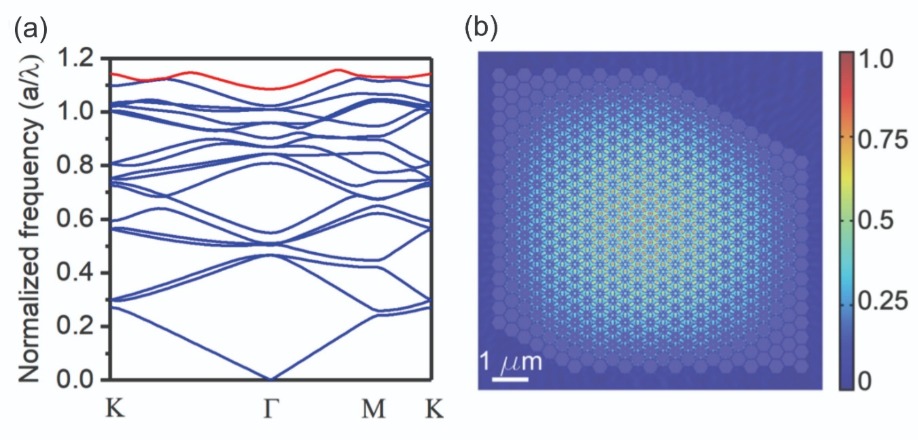
Figure 4. (a) Band structure of the designed photonic crystal structure targeted to operate at 370 nm with a lattice constant of 400 nm. The Γ point in the band in red colour is the designed operation wavelength. (b) The design of the irregular shaped nanowire photonic crystal, acting as a topological high-Q resonator, and the mode profile with a Q factor of 11,460. For more details, see: B. H. Le et al. Opt. Express 27 5843 (2019)
Topological resonatorsThe performance of the UV laser diodes is held back by the lack of a high-reflectance mirror for optical feedback. Its absence results in a high threshold and severe heating.
One solution is to form a defect-free photonic nanocrystal structure that functions as a topological resonator with a high quality factor. Note that this architecture does not need extra mirrors for optical feedback. Designs with an arbitrary irregular shape can exhibit a high quality-factor resonance at the G point, a feature that is essential for the robustness of device operation.
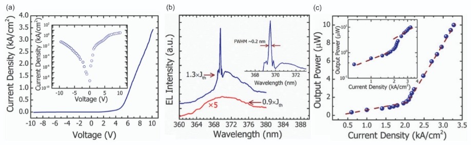
Figure 5. (a) Current-voltage characteristics of the photonic nanocrystal laser. Inset: Current-voltage characteristics displayed on a semi-log scale. (b) Emission spectra of photonic nanocrystal lasers below (red) and above (blue) threshold current. (c) Variation of output with injection current. Inset: Variation of output with injection current displayed on a log scale. For more details, see: B. H. Le et al. Opt. Express 27 5843 (2019)
We have undertaken simulations of irregular photonic crystals with a lattice spacing of 400 nm, and a separation between the nanocrystals of 36 nm (see Figure 4). These calculations suggest a Q-factor of over 11,000. This is a high value that has encouraged us to produce a laser diode with this architecture. The current-voltage characteristics of this device, featuring a topological resonator based on an AlGaN nanowire photonic crystal structure, include a turn-on voltage of only 4 V and a very low reverse bias leakage current (see Figure 5(a)). When operating at room-temperature, as the current increases from below to above threshold, a sharp lasing peak with a linewidth of about 0.2 nm emerges from the broad spontaneous emission (see Figure 5(b)). We have also studied the variation in output with injection current, with results revealing an unambiguous lasing threshold of 10.6 mA (see Figure 5(c)).Our efforts show that AlGaN nanocrystals have many desirable properties, including negligible defects and dislocations, highly efficient p-type conduction, and efficient light extraction. All these strengths are difficult to realise with conventional AlGaN planar structures. Further work is now needed to develop efficient mid- and deep-UV optoelectronic devices, including LEDs and laser diodes, that are hampered by standard device architectures.
X. Liu et al. IEEE Photon. J. 10 1 (2018)
X. Liu et al. Opt. Express 25 30494 (2017)
X. Liu et al. Photonics Res. 7 B12 (2019)
N. H. Tran et al. Appl. Phys. Lett. 110 032102 (2017)
B. H. Le et al. Opt. Express 27 5843 (2019)


