GaN Systems and ON Semi Demo latest GaN technology

Half-Bridge evaluation board makes it easier to design with GaN
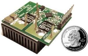
GaN Systems and ON Semiconductor have announced the availability of a high-speed, half-bridge GaN daughter board using GaN Systems’ 650 V, 30 A GaN E-HEMTs and ON Semiconductor’s award-winning NCP51820 high speed gate driver evaluation board.
This evaluation board is developed for existing and new PCB designs and allows designers to evaluate GaN in existing half−bridge or full−bridge power supplies. The kit has a reduced component count in an ultra-small 25mm x 25mm layout, minimising PCB board space. Features, which include 1+ MHz operation and a 200 V/ns CMTI rating, provide increased power density and improved performance with fast-switching GaN power transistors.
Benefits include reductions in power losses, weight, size (up to 80 percent in layout size), and system costs (up to 60 percent BOM cost savings) and ideal in applications such as AC-DC adapters, data center power supplies, PV inverters, energy storage systems, and Bridgeless Totem Pole topologies. This solution is one of many upcoming GaN-based power system solutions both companies are developing.
“The expansion of the GaN components ecosystem including driver ICs such as our NCP51820 remove design barriers and take advantage of the numerous benefits that GaN E-HEMTs provide,” stated Ryan Zahn, director of marketing at ON Semiconductor. “With rising interest and adoption of GaN, we look forward to continued collaboration with GaN Systems in supporting and meeting the new power requirements taking place across many industries.”
“The new evaluation board developed in collaboration with ON Semiconductor makes it easier and more cost effective to design with GaN – opening the door for smaller, lighter, and more efficient power converters,” said Charles Bailley, senior director, Worldwide Business Development at GaN Systems. “This collaboration signals the innovation not only happening with end products designed with GaN but in components, design tools, and reference designs that optimise the use of GaN.”


