US team models GaN thermal conductivity

University of Illinois researchers propose new empirical model to describe how thermal conductivity of GaN is affected by dislocation density
GaN materials are critical for energy conversion, communication, and sensing. But despite all the material advantages, current mainstream GaN photonic and electronic devices are limited by the thermal heat extraction.
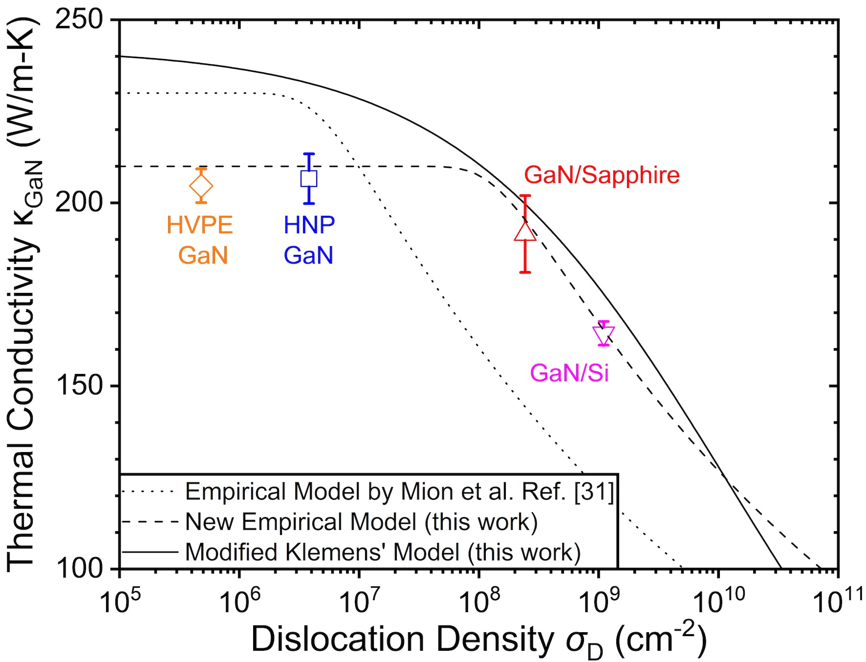
In the recent issue of Journal of Applied Physics, a University of Illinois research team led by Cam Bayram investigates the thermal conductivity of technologically important GaN materials: Hydride vapour phase epitaxy grown GaN (HVPE GaN), high nitride pressure grown GaN (HNP GaN), and MOCVD grown GaN on sapphire (GaN/sapphire) and on Si (111) (GaN/Si).
The team was able to report a systematical thermal conductivity study of GaN materials with various dislocation densities. Thermal conductivities were measured by time-domain thermoreflectance technique, dislocation densities were measured by cathodoluminescence and X-ray diffraction, and impurity densities were measured by secondary mass ion spectroscopy to complement the analysis.
Using the experimental data, the team proposes a new empirical model to describe how thermal conductivity of GaN is affected by the dislocation density. They also propose a modification in Klemens’ model to explain the experimental thermal conductivity – dislocation density relationship. The figure above demonstrates how thermal conductivity of GaN is affected by the dislocation density
'Impact of dislocations on the thermal conductivity of GaN studied by time-domain thermoreflectance' by K. Park and C. Bayram; J. Appl. Phys. 126, 185103 (2019).


