
Researchers develop high-Power GaN VLEDs on Silicon
Optimised metallisation scheme with SiO2 current blocking layer could deliver cheaper and reliable next-generation solid-state lighting devices
Researchers from Wuhan University in China and the LED company Changelight have reported developing high power, reliable GaN-based vertical LEDs (VLEDs) on 4-inch p-type silicon substrate. They achieved this using an optimised metallisation scheme with an SiO2 current blocking layer. In addition, by surface texturing the emitting surface of the VLED with KOH wet etching, they say they have boosted the light extraction efficiency.
“We may have found access to more cheap and reliable next-generation solid-state lighting devices," said Shengjun Zhou who led the Wuhan team.
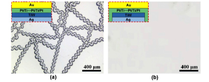
Deposited metallisation schemes can buckle and delaminate in humid environments, which is a major concern for the reliability of VLEDs. In the study, published in Optics Express, the researchers demonstrated that the metallisation reliability can be improved by depositing Pt/Ti protective layers surrounding the Ag/TiW films to protect the interface from environmental humidity.
Figure 1 above shows optical microscope images of different metallisation scheme designs suffering from moisture in the air: (a) Conventional multilayer metallisation stacks without lateral protection; (b) Multilayer metallisation stacks with Pt/Ti capping layers surrounding the Ag/TiW films.
Light absorption by the metal contacts is one source of optical loss sources in LEDs. However, most of current is crowded in proximity of the electrodes due to the non-ideal conductivity of the semiconductor layers, leading to a localisation of emission around the electrode pads.
The researchers show that 'current crowding' can be significantly relieved by the insertion of a SiO2 current blocking layer under the p-electrode. A more uniform current distribution with the application of SiO2 current blocking layer was demonstrated using simulation results.

Figure 2. (a) Optical microscope images of the L-LED and V-LED. (b) Simulated current density distribution in the active layers of L-LED, V-LED and V-LED with SiO2 CBL. (c) Calculated current density profiles along the dotted line in (b).
The researchers also took advantage of KOH wet chemical etching to texture the emitting surface of VLEDs for a higher light extraction efficiency. Highly integrated surface textures consisted of periodic hemispherical dimples and hexagonal pyramids was formed after wet etching using KOH solution. Finite difference time domain (FDTD) simulation reveal such surface morphology not only reduces the Fresnel reflection but also scatters the light outward with a broad distribution, enabling a higher light extraction efficiency.
'High-power and reliable GaN-based vertical light-emitting diodes on 4-inch silicon substrate' by Shengjun Zhou et al; Optics Express, Vol. 27, No. 20, 30 Sep 2019


