
2D materials: the future for scaling of logic and memory?
Imec makes ultra-scaled FETs with 2D semiconductor channels
At this year’s IEEE International Electron Devices Meeting (Dec 7-11 2019), Belgian research hub Imec is presenting an in-depth study of scaled transistors with MoS2 that shows best device performance to date for such materials.
MoS2 is a 2D compound semiconductor that can be grown in stable form with nearly atomic thickness and atomic precision. Imec synthesised the material down to monolayer (0.6nm thickness) and fabricated devices with scaled contact and channel length, as small as 13nm and 30nm respectively. These very scaled dimensions, combined with scaled gate oxide thickness and high K dielectric, have how some of the best device performances so far, according to Imec.
By studying these transistors, scientists can learn about fundamental device properties and build TCAD model to discover new ways to improve performance.
Imec says its results confirm the potential of 2D-materials for extreme transistor scaling – benefiting both high-performance logic and memory applications. Theoretical studies recommend 2D materials as the perfect channel material for extreme transistor scaling as only little short channel effects are expected compared to today's silicon-based devices. Hints of this potential have already been published with one-of-a-kind transistors built on natural flakes of 2D materials.
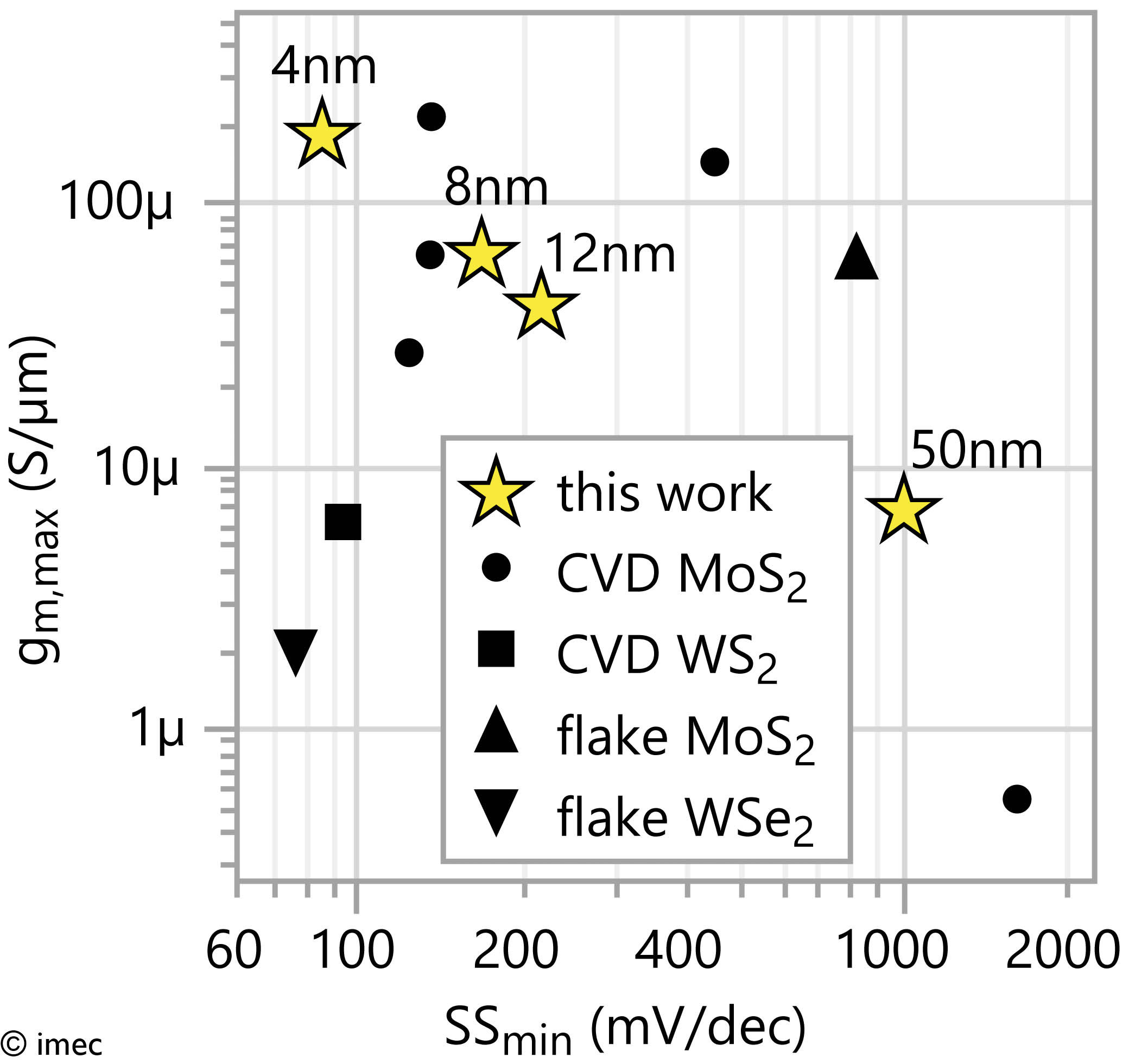
For the first time, Imec has tested these theoretical findings through a comprehensive set of 2D-materials-based transistor data. The devices with the smallest footprint have a channel length of 30nm and <50nm contact pitch. ON current as high as 250µA/µm has been demonstrated with 50nm SiO2 gate dielectric. On current of ~ 100 µA/µm and an excellent SSmin of 80mV/dec (for VD =50mV) have been demonstrated with 4nm HfO2 in a backgated configuration.
The figure above shows the gmmax and SSmin performance of Imec’s devices with 4nm, 8nm, 12nm HfO2 and 50nm SiO2 compared to literature.

Figure 2: TEM pictures showing (a) 3 monolayers MoS2 channel, with contact length 13nm and channel length 29nm Transfer characteristics have improved sub-threshold swing (SS) with thinner HfO2.
Imec says the device performance is not impacted by contact length scaling, confirming that carriers are injected from the edge of the contact metal directly into the channel, in line with TCAD simulations. The work confirms that TCAD models capture large parts of device physics and guide experimental validation and mapping the application space. Part of the paper that is presented at IEDM, is dedicated to setting the path for device optimisation for reaching Si-like performance targets.

Figure 3: Transfer characteristics have improved sub-threshold swing (SS) with thinner HfO2.
“Although still an order of magnitude away from silicon transistors, we have brought our MOSFET devices into a realm where they show promising performance for future logic and memory applications”, says Iuliana Radu, director of Exploratory and Quantum Computing Imec. “To bridge this order of magnitude, we have identified a path of systematic improvements such as a further reduction of the gate oxide thickness, the implementation of a double-gated architecture, and further reduction of channel and interface defects. We are transferring this insight to our 300mm-wafer platform for transistors with 2D materials, which was announced at last year’s IEDM.”
“As a world-leading research and innovation hub, it is Imec’s role to push device scaling towards the ultimate limit. We are tackling this challenge by investigating different scaling options, providing optimal projections, and guiding the industry to adopt the proposed solutions, stated Luc Van den hove, Imec CEO. “Our partners expect us to lead the way and to support them in realising their roadmaps by demonstrating the potential of innovative concepts and novel materials. This is why I am so thrilled we have demonstrated excellent performance in ultra-scaled devices with 2D materials, and a credible path to further improvements aiming at mass production in industrial 300mm fabs.”


