Loading...
News Article

RENA acquires US-based MEI

News

Aims to diversify wet-chemical surface treatment portfolio and approach the US semiconductor market

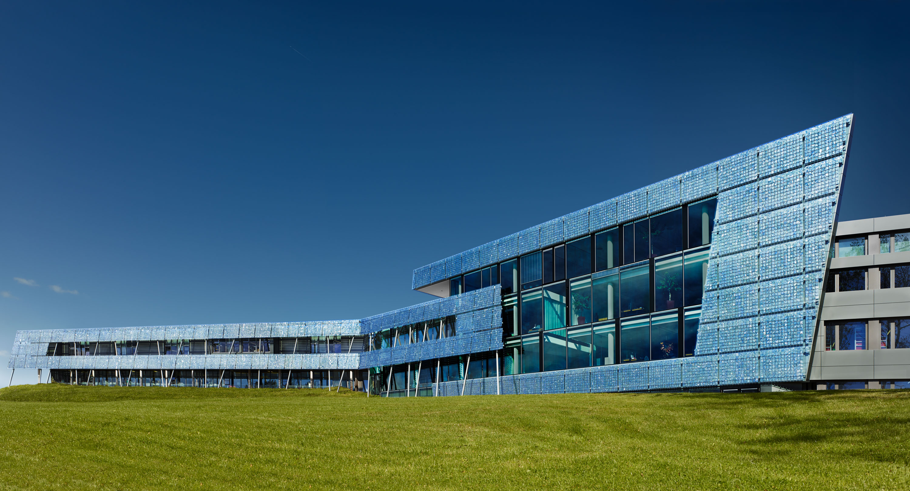
Germany-based RENA Technologies GmbH (HQ pictured above) is acquiring MEI LLC headquartered in Albany, Oregon, to combine both companies’ individual strengths in the high-end semiconductor market.

This investment is part of RENA's strategy to diversify its wet-chemical surface treatment product and service portfolio and approach the US semiconductor market.

RENA’s main markets are Europe and Asia while MEI has an established track record within the US high-tech semiconductor sector. Synergies can be found in the regional distribution of both companies’ customer base as well as their local service organisations, which allows them to offer a complete service portfolio. Together, the companies can cover all wet-chemical process steps of semiconductor processing, from best-in-class prime wafer processing to state-of-the-art MEMS, SiC and semiconductor processing including Batch Immersion, Batch Spray, and Single-wafer applications.

“MEI’s and RENA’s product portfolios complement each other extremely well” said Peter Schneidewind, CEO of RENA, “We strongly value the expertise of our new colleagues from MEI and are delighted to be able to offer our customers comprehensive solutions for semiconductor wet-processing equipment on a worldwide scale.”

“With a large number of orders in our backlog, we’re happy to join RENA Group, which provides us with a range of opportunities in regard to global market access and synergies in services, R&D, and production. This gives MEI the chance to advance to the next level globally,” added Ed Jean, CEO of MEI.

“We are absolutely convinced, that this combination brings superior value for our customers through an extended product portfolio and our joint global service team,” both CEOs summarised.

SiC MOSFETs: Understanding the benefits of plasma nitridation
Wolfspeed reports Q2 results
VueReal secures $40.5m to scale MicroSolid printing
Mitsubishi joins Horizon Europe's FLAGCHIP project
Vishay launches new high voltage SiC diodes
UK team leads diamond-FET breakthrough
GaN adoption at tipping point, says Infineon
BluGlass files tuneable GaN laser patents
QD company Quantum Science expands into new facility
Innoscience files lawsuit against Infineon
Riber revenues up 5% to €41.2m
Forvia Hella to use CoolSiC for next generation charging
Photon Design to exhibit QD simulation tool
Ortel transfers CW laser fabrication to Canada
Luminus adds red and blue multi-mode Lasers
PseudolithIC raises $6M for heterogeneous chiplet tech
Mesa sidewall design improves HV DUV LEDs
IQE revenue to exceed expectations
'Game-changing' VCSEL system targets clinical imaging
German start-up secures finance for SiC processing tech
Macom signs preliminaries for CHIPS Act funding
IQE and Quintessent partner on QD lasers for AI
EU funds perovskite tandems for fuel-free space propulsion
EU to invest €3m in GeSi quantum project
Transforming the current density of AlN Schottky barrier diodes
Turbocharging the GaN MOSFET with a HfO₂ gate
Wolfspeed launches Gen 4 SiC MOSFET technology
Report predicts high growth for UK's North East
Element Six unveils Cu-diamond composite
SemiQ launches hi-rel 1700V SiC MOSFETs
Lynred to exhibit Eyesential SWIR sensor for machine vision
Thorlabs buys VCSEL firm Praevium Research
×
Search the news archive

To close this popup you can press escape or click the close icon.
Logo
x
Logo
×
Register - Step 1

You may choose to subscribe to the Compound Semiconductor Magazine, the Compound Semiconductor Newsletter, or both. You may also request additional information if required, before submitting your application.


Please subscribe me to:


You chose the industry type of "Other"

Please enter the industry that you work in: