
Researchers develop High-Efficiency Flip-Chip GaN LED
Team from Wuhan University and Changelight use Ohmic and Bragg reflectors with 3D vias to improve power performance
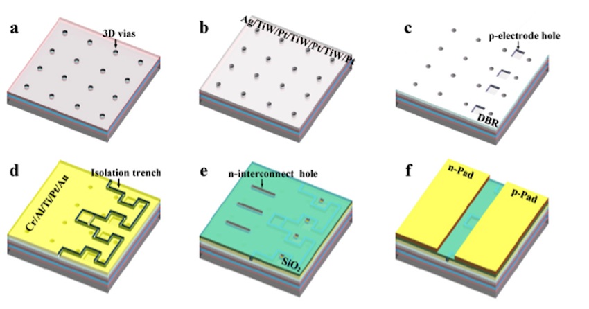
Researchers from Wuhan University in China, in collaboration with the LED company Changelight, have reported developing highly efficient GaN-based high-power flip-chip LEDs (FCLEDs). They achieved this by using a highly reflective Ag/TiW/Pt/TiW/Pt/TiW/Pt ohmic reflector, a dielectric TiO2/SiO2 distributed Bragg reflector (DBR), and 3D vias. The illustration (above) shows the fabrication process flow.
In the study, published in Optics Express, the researchers describe the ohmic contact mechanism between Ag and p-GaN using first-principles calculations. A high temperature annealing process at ~600degC is necessary to obtain good Ohmic contact between Ag and p-GaN. However, the agglomeration of Ag-based Ohmic reflector in high-temperature annealing process leads to degradation in both electrical and optical properties, which become the main obstacle to obtaining high-quality Ag-based ohmic contacts in FCLEDs.
To preserve the highly reflective Ag-based Ohmic contacts, the researchers developed a thick diffusion barrier consisted of TiW and several Pt interlayers, which effectively relax the tensile stress and thus eliminate cracking during thermal annealing.
Light absorption by the metal contacts is one source of optical loss sources in LEDs. However, most of current is crowded in proximity of the electrodes due to the non-ideal conductivity of the semiconductor layers, leading to a localisation of emission around the electrode pads. The researchers designed uniformly distributed 3D vias for electrodes connection, which improve the current spreading over the entire active region and reduce the loss of active areas. In addition, the inclined sidewalls of the 3D vias were covered by insulating TiO2/SiO2 double DBR stacks, which minimise the light absorption by the opaque n-electrodes and provide a higher light extraction efficiency.
'Highly efficient GaN-based high-power flip-chip light-emitting diodes' by Shengjun Zhou et al; Optics Express, Vol. 27, Issue 12, pp. A669-A692 (2019).


