
Sanan Appoints Plextek RFI for 5G GaAs MMIC Design
Plextek RFI demonstrates 5G mmwave PA reference design on Sanan technology
Sanan IC, a pure-play Chinese wafer foundry, has announced its collaboration with Plextek RFI, a UK-based design house specialising in RF microwave and millimeter-wave circuit designs, as an authorsized resource for GaAs MMIC design services in the emerging 5G market.
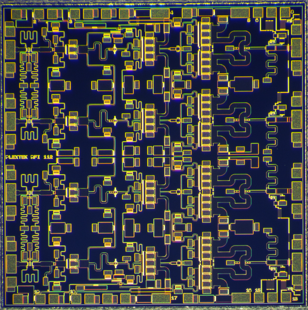
This partnership has already been demonstrated by the recent design by Plextek RFI of a single-chip surface mount packaged 4-channel 5G millimeter wave power amplifier (PA) for the 28GHz spectrum using Sanan IC’s P15EP1 0.15µm 6 inch GaAs E/D pHEMT process technology.
The reference design was displayed and presented by Plextek RFI at the recent Automated RF and Microwave Measurement Society (ARMMS) Conference held in Bedfordshire, UK.
“As the 5G infrastructure market expands from sub-6GHz into the millimeter-wave spectrum, RF front-end design activities for the associated telecoms equipment are naturally increasing,” said Raymond Cai, CEO of Sanan IC. “We are pleased to have Plextek RFI as an authorized design services partner, to assist our customers worldwide in augmenting their GaAs IC design and development resources with RF engineering expertise. We anticipate that our newly launched P15EP1 E/D pHEMT GaAs process will be widely adopted in high-performance millimeter-wave applications, particularly in the 5G space.”
“The roll-out of 5G infrastructure has generated demand for a variety of millimeter-wave RF front-end architectures and topologies that require high performance GaAs IC designs,” commented Plextek RFI CEO Liam Devlin. “We are delighted to provide our clients innovative solutions and design options to address these requirements, as demonstrated by our compact, multi-channel power amplifier reference design on Sanan IC GaAs technology. We expect to build on this success by leveraging other Sanan IC GaAs processes and exploiting its future roadmap for high-performance, high integration, and high quality RF designs.”
The company’s P15EP1 process is a high-performance 6inch GaAs pHEMT technology, integrated with E-mode, 0.15µm gate length transistors which have an Ft of 85GHz and Fmax of 155GHz. The process is suitable for millimeter-wave PA and LNA designs, offering high gain, low noise figure, and wide bandwidth, and can be combined with 0.5µm E-mode/D-mode devices for single-die logic implementation.
This technology platform provides up to 3 metal interconnect layers, with 12 mask layers with and a back lapping thickness of 75µm. The P15EP1 process is part of the P15 family of GaAs technologies, which can provide other options such as D-mode transistors, PIN diodes for switches and limiters, and which will be augmented later next year with a lower process node for higher frequency support.


