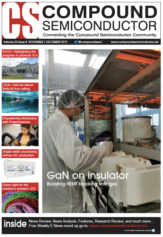
Insulating interlayer boosts the breakdown voltage
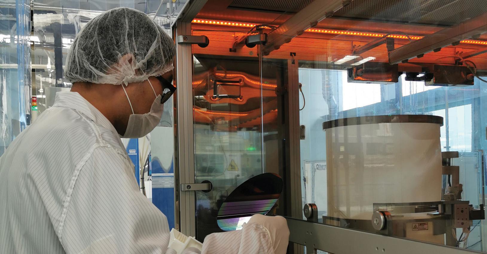
HEMTs exceed the breakdown limit imposed by the epilayer when an insulator is inserted between GaN and silicon
BY ZHIHONG LIU, HANLIN XIE AND KWANG HONG LEE FROM SINGAPORE-MIT ALLIANCE FOR RESEARCH AND TECHNOLOGY, CHUAN SENG TAN AND GEOK ING NG FROM NANYANG TECHNOLOGICAL UNIVERSITY, AND EUGENE FITZGERALD FROM MASSACHUSETTS INSTITUTE OF TECHNOLOGY
GaN has many great attributes, including a wide bandgap, a substantial critical electric field, and a high density for its polarization-induced two-dimensional electron gas. It is these qualities that are behind the high performance of the GaN HEMT. This transistor outperforms rivals made from silicon, and enables the construction of power converters that combine a low power loss with a high power conversion efficiency and a high operation frequency.
To make GaN power diodes and transistors even more competitive with their silicon-based counterparts, the cost of these products must fall. One promising option is to manufacture these devices from 200 mm GaN-on-silicon wafers, as this enables a low substrate cost and high-volume production at mature silicon foundries. Much progress has been made on this front, including some commercial production of these wide bandgap HEMTs from 200 mm GaN-on-silicon epiwafers.
However, with this technology, there are concerns related to the breakdown voltage of the transistor. HEMTs, like other lateral power devices, have a breakdown voltage that increases with its gate-to-drain distance. Drawing on this, a team from Panasonic Corporation has realised a breakdown voltage of just over 10 kV, using a gate-to-drain distance of 125 µm. However, the substrate for this record-breaking feat is not silicon, but sapphire. It’s a good choice – as would be SiC – because it allows the widening of the gate-to-drain distance to boost the blocking voltage. That’s not the case with silicon, due to vertical breakdown in the GaN epilayer, leading to a leakage current flowing through the conductive silicon substrate (see Figure 1). For this compromised material combination, the maximum achievable breakdown voltage is governed by the GaN epilayer thickness.
To try and increase the breakdown voltage of the GaN-on-silicon HEMT, much effort has been directed at improving the growth techniques, to enable a thicker GaN buffer on the silicon substrate. Accomplishing this is far from easy, due to the severe issues of wafer crack, bow and even breakage. All stem from the large lattice mismatch and the large thermal expansion coefficient discrepancy between the silicon substrate and GaN epilayers. These differences have a tremendous impact on large-size wafers, such as those with a 200 mm diameter. For this size wafer, until recently the breakdown voltage of the GaN HEMT has been restricted to below 1900 V, with the best results coming from strutures with a 4.5 µm GaN epilayer thickness.
Several technologies have been developed to try and overcome this limitation. At MIT, Tomas Palacios’ team have transferred the GaN HEMT epilayers from the silicon substrate to glass, in an attempt to increase the breakdown voltage of the lateral device. This paid dividends, increasing breakdown from around 600 V to 1.5 kV, and offering experimental proof that the silicon substrate is the root cause of the breakdown voltage saturation in HEMTs with a gate-to-drain distance that’s beyond a certain value. However, the switch to glass is not a great solution – it has a poor thermal conductivity, and it is not compatible with silicon CMOS foundries.
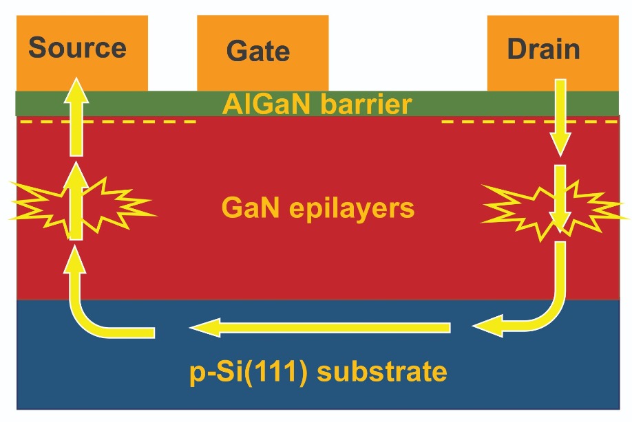
Figure 1. After the GaN epilayers are vertically broken down in a conventional GaN-on-silicon HEMT, current flows through the conductive silicon substrate.
Other groups have enjoyed some success by locally removing the silicon substrate. It’s an idea that has been proposed by Puneet Srivastava at co-workers from imec, and pursued by Farid Medjoub’s group at IEMN that have realised breakdown voltages of 3 kV.Again, there is a price to pay for this triumph. In this case, substrate removal leads to mechanical stability issues, both for large-area power devices and for large-size GaN-on-silicon wafers. In addition, thermal spreading is compromised, with the loss of part of the silicon substrate limiting the paths of heat spreading, leading to an increase in thermal resistance.
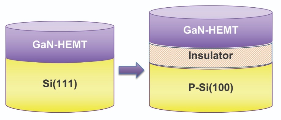
Figure 2. GaN-on-insulator (GNOI)-on-silicon wafers can break through the limit of breakdown voltage caused by GaN epilayer vertical breakdown. This is accomplished by adding an insulating layer between the GaN epilayers and the silicon substrate to enhance the vertical breakdown voltage.
To avoid issues associated with either the use of glass or with substrate removal, our team from the Singapore-MIT Research and Technology Alliance, Nanyang Technology University and Massachusetts Institute of Technology is pioneering a different approach – the use of a GaN-on-insulator (GNOI)-on-silicon structure (see Figure 2). Unveiled at the VLSI Symposium 2019, our novel architecture avoids the need for thick GaN epilayers by using wafer-bonding to insert an additional insulator between the silicon substrate and the device layers.Our approach holds many advantages. Using large silicon wafers, we can process our material in silicon foundries; we can remove the original transition layer that is hampered by numerous dislocations and poor thermal conductivity, thereby improving device reliability and heat dissipation; and after high temperature GaN growth, we can replace the original, fragile silicon substrate with a new one with good hardness – this reduces the probability that a wafer breaks as it passes through the line, leading to higher yield.
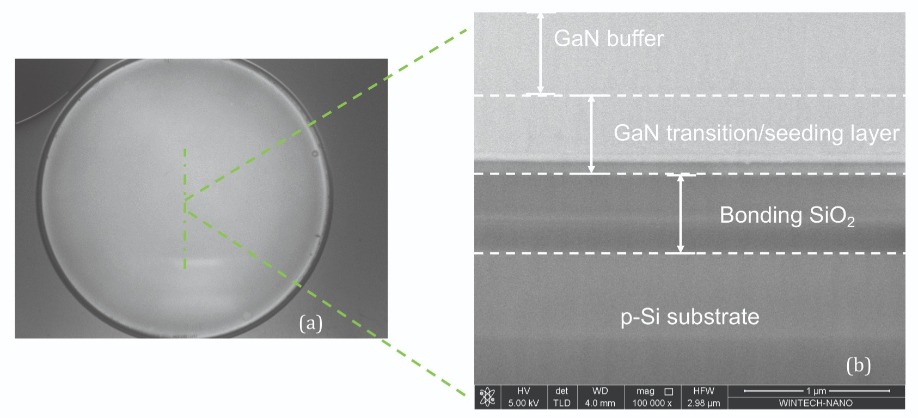
Figure 3. (a) Infrared transmission image of the prepared GNOI wafer. There are no obvious bubbles formed; (b) scanning electron microscopy image of the cross-section of the GNOI wafer.
Inserting the insulatorFabrication of our novel HEMTs begins by preparing a 200 mm GaN-on-silicon (111) wafer and a silicon handling substrate. SiO2 is deposited on the front side of both of them, followed by densification of this oxide, before chemical mechanical polishing reduces surface roughness. After this, the surfaces are cleaned, treated with plasma activation, and bonded together. Subsequent high-temperature annealing strengthens this bond.
To enable insertion of the insulator, the original silicon (111) substrate for the growth of the GaN epilayers is removed. This exposes the back side of the GaN epilayers – in our case, the N-polar side – so that it can be bonded to a new p-silicon (100) substrate. Similar to the first bonding process, after SiO2 deposition, densification, chemical-mechanical polishing and surface activation, the GaN-on-silicon handling wafer and the new p-silicon (100) wafer are bonded together. Finally, the silicon handling substrate and the bonding material are removed, to expose the GaN front surface (Ga-polar) and realise a GNOI-on-silicon wafer (see Figure 2).
We have scrutinised the material quality of our heterogeneous structure within a variety of techniques. Infrared transmission images of our 200 mm GNOI-on-silicon wafer reveal that there are no visible bubbles at the bonding interface (see Figure 3 (a)), and scanning electron microscopy shows that there are clear interfaces between the GaN, SiO2 and silicon.
According to Hall measurements, the density and mobility of the two-dimensional electron gas are 8.7 x 1012 cm-2 and 1930 cm2 V-1s-1, respectively. Comparing these values to those for GaN-on-silicon structures shows that our processes for producing our GaNOI-on-silicon wafers do not impact the electrical characteristics of the GaN heterostructure.
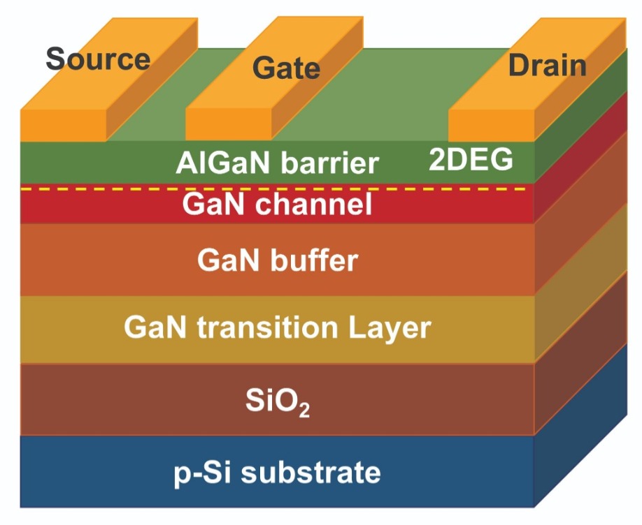
Figure 4. A fabricated HEMT on a GNOI-on-silicon wafer.
Evaluating performanceTo see if our GNOI architecture can fulfil its promise, we have fabricated GaN HEMTs from a small piece of a 200 mm GaNOI-on-silicon wafer (see Figure 4 for a diagram of our GaN HEMT structure). These transistors have been formed using a standard fabrication process flow for GaN HEMTs. After device isolation, realized through a mesa plasma etch, we create ohmic contacts from a Ti/Al/Ni/Au metal stack that is annealed at 775 °C. Measurements reveal that the ohmic contact resistance is 0.5-0.7 Ω-mm. Fabrication of these transistors is completed with the construction of Schottky gate contacts, formed by
Ni/Au metallization and post-gate-annealing at 400 °C for 10 min under nitrogen gas. Note that no field plates are used in these devices. To benchmark them, we have also made GaN HEMTs from a piece of 200 mm GaN-on-silicon wafer, using an identical process.
Measurements using the well-known FATFET technology have uncovered the 2DEG drift mobility in both forms of HEMT. The insertion of the insulator has no noticeable impact, with mobilities for both types of transistor in the range 1900-2100 cm2 V-1s-1.

Figure 5. (a) Output (Id-Vd) and (b) transfer (Id-Vg) characteristics of a HEMT on a GaN-on-silicon substrate with Lgs/Lg/Lgd=2/2/14 µm; (c) Output (Id-Vd) and (d) transfer (Id-Vg) characteristics of a HEMT on GNOI-on-silicon substrate with Lgs/Lg/Lgd=2/2/14 µm.
We have also measured the DC characteristics of both types of HEMT, considering devices with a gate-to-source separation of 2 µm, a gate length of 2 µm, and a gate-to-drain distance of 14 µm. Plots shown in Figure 5 reveal that for the GNOI-on-silicon device, the maximum drain current is 508 mA/mm, the on-resistance is 8.8 Ω mm, the maximum transconductance peaks at 140 mS/mm, and the threshold voltage is -2.85 V. For the GaN-on-silicon variant, values are only slight different – the figures are 576 mA/mm, 11.0 Ω mm,147 mS/mm, and -2.37 V.After grounding the silicon substrates and applying a positive bias to an ohmic pad fabricated on the top AlGaN/GaN heterostructure, we have measured the vertical breakdown voltage (see Figure 6 for a plot of the vertical leakage current at different values for the bias). The vertical breakdown voltage of the GNOI-on-silicon wafer is 1416 V – an improvement of around 430 V compared with the GaN-on-silicon wafer.
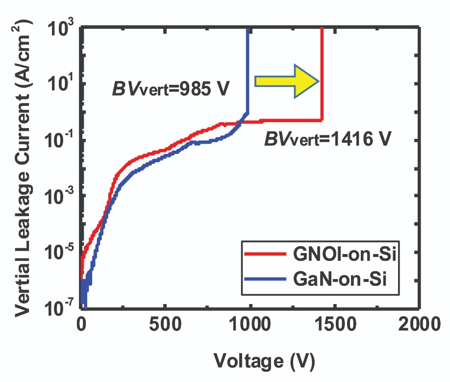
Figure 6. Vertical leakage current versus the voltage biased on an ohmic contact pad on GNOI-on-silicon and GaN-on-silicon wafers with substrate grounded.
With substrates ‘floating’, we have measured three-terminal off-state breakdown characteristics (see Figure 7). The off-state breakdown voltage is defined at 1 mA/mm, a value at which hard breakdown occurs. Plots clearly show that as the gate-to-drain distance increases, the breakdown voltage increases initially, before saturating – for the GNOI-on-silicon HEMTs, the on-set of this plateau is at 14 µm, while for the control it starts at 9 µm. Causes for failure are a combination of vertical breakdown of the GaN epilayers and/or SiO2, and a current flow through the conductive silicon substrate.Inserting the insulator between GaN and the silicon substrate delivers a substantial improvement to the breakdown voltage. It increases by about 700 V, to around 2 kV. The maximum breakdown can be as high as 2200 V, realised for a device with a gate-to-drain distance of 35 µm.
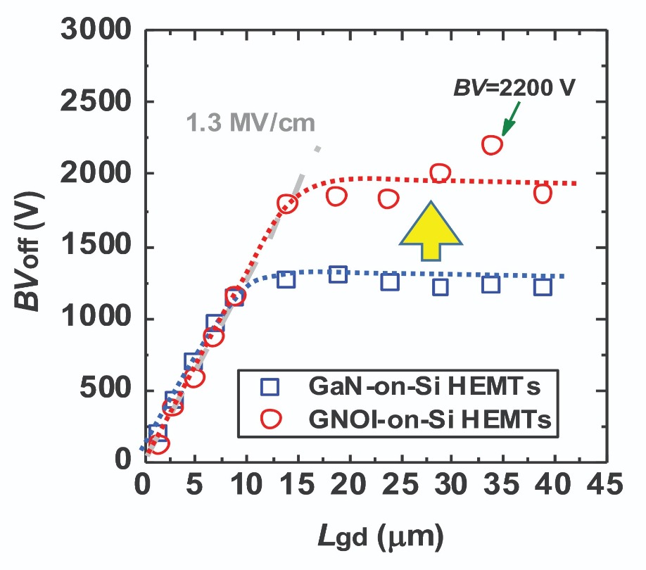
Figure 7. Three-terminal off-state breakdown characteristics of the devices with different gate-to-drain length on (a) GaN-on-silicon wafer and (b) GNOI-on-silicon wafer. The substrate was floating. Breakdown voltage (BVoff) was defined at Ids=1 mA/mm.
We have benchmarked our devices, judging them in terms of total GaN epilayer thickness, against other reports of HEMTs made from 200 mm GaN-on-silicon wafers. Our highest voltages of 2.2 kV breaks new ground, beating the previous record of 1900 V, reported by IQE and using 4.5 µm GaN epilayers (see Figure 8). These figures actually undervalue the benefits wrought with the insulator. Compare results for the same epilayer thickness – that is, 3.2 µm – and the breakdown voltage is 900 V higher with the GNOI structure.Another important consideration is the specific on-resistance, and how it relates to the breakdown voltage. Again, our devices are raising the bar for what is possible (see Figure 8(b)). For HEMTs made from 200 mm GaN-on-silicon wafers, one figure-of-merit is a record 1.87 GW/cm2.
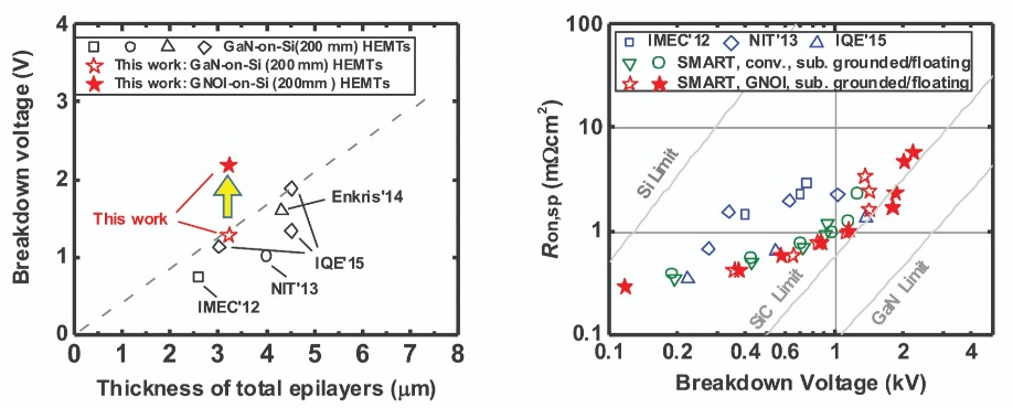
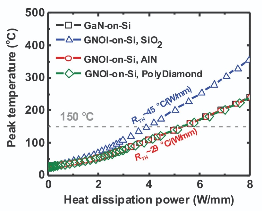
Figure 8. (a) State-of-the art BVoff versus the total GaN epilayer thickness for 200 mm GaN-on-silicon wafers. (b) Reported Ron,sp as a function of BVoff for HEMTs on 200 mm GaN wafers. In this work a record FOM (BV2/Ron,sp) value of 1.87 GW/cm2 has been achieved.
Solution of the thermal issueOne weakness of our GNOI-on-silicon wafers is the poor thermal conductivity of the SiO2 layer that provides the wafer-bonding insulator. To assess the impact of the insulating layer’s effect on the device’s thermal performance, we have undertaken electrothermal simulation with a Silvaco TCAD tool. For this work, we have used thermal conductivity values of 0.3 W/cm-K for the AlGaN barrier, 1.6 x (300/T)1.4 W/cm-K for the GaN buffer, 0.1 W/cm-K for the GaN transition layer, 0.012 W/cm-K for the SiO2 bonding material, and 1.48 x (300/T)1.65 W/cm-K for the silicon substrate.
Options for combatting the performance of HEMTs made from GNOI-on-silicon wafers include replacing the low thermal conductivity SiO2 bonding material with one that is superior on this front. Candidate materials include AlN and polycrystalline diamond.
To evaluate the benefits of these materials, we have carried out simulations, using values of 1.13 W/cm-K for the thermal conductivity of 700 nm AlN, and 2.3 W/cm-K for 700 nm of polycrystalline diamond. According to the calculations, the addition of either AlN bonding material or polycrystalline diamond bonding material trims the thermal resistance of the device from 45 °C(W/mm) to 29 °C(W/mm).
Superior thermal management holds the key to higher powers. If the channel temperature must be no more than 150 °C, the allowable power increases from 3.9 W/mm for the GNOI-on-silicon wafer with SiO2 bonding material to 5.3 W/mm with AlN bonding material and 5.4 W/mm with polycrystalline diamond bonding material. This is a significant improvement, indicating that the thermal issue created by the SiO2 bonding material can be addressed with either AlN or poly-crystalline diamond.
In short, it is clear that introducing new materials to the GaN-on-silicon HEMTs improves ther performance of this transistor. Inserting SiO2 propels the breakdown voltage to a new high, and increases other figures-of-merit; and the addition of bonding materials with a higher thermal conductivity than SiO2 prevents any compromise to thermal management. This shows that more powerful HEMTs that can keep their cool are within our grasp.
Z. Liu et al. Proc. of VLSI tech., 2019
B. Lu et al. IEEE Electron. Dev. Lett. 31 951 (2010)
E. A. Fitzgerald et al. ECS Trans. 75 31 (2016)
Y. Zhang et al. IEEE Tran. Electron Dev. 60 2224(2013)


