
LEDs: GaN-on-silicon finds its calling

Processing GaN-on-silicon epiwafers through a dedicated silicon line offers a very attractive approach to making microLED displays
BY RICHARD STEVENSON
The GaN-on-silicon LED has always attracted much attention. It grabbed the headlines at the start of this decade when Bridgelux billed the technology as the one to slash the cost of LED lighting. Manufacturing costs for LED chips would plummet, thanks to a switch to cheaper, larger wafers, and the opportunity to process devices in underutilised, fully depreciated 200 mm silicon lines. But instead, with the help of subsidies and a significant fall in the price of the sapphire substrate, it has been the companies from China that have flooded the market, by slashing the cost of conventional chips.
It’s not just Bridgelux that has suffered from this unexpected twist. Hopes have also been dashed at the UK firm Plessey. Back in 2012, it acquired GaN-on-silicon technology from CamGaN, a spin-off of the University of Cambridge. After establishing the process at its site in Plymouth, it spent several years trying to turn a profit in the LED lighting market. Efforts focused on finding a niche where it could make an impact. Products were launched for spotlights, for circadian lighting and for horticulture, but none of these ventures realised significant success.
So does this mean that the GaN-on-silicon LED is never going to succeed? Absolutely not. All that’s needed is to find an applications that will really benefit from this form of LED. And under the current leadership, including President Michael Lee, who joined Plessey in 2017 and leads business and corporate development, the company is doing just that. It has identified displays, made from microLEDs, as a fantastic fit for this technology, and it is now focused entirely on this lucrative sector.
For this class of application, the GaN-on-silicon LED has a critical advantage over its more common, sapphire based cousin: as the size of the emitter reduces, its performance pulls ahead. That’s because the light extraction is higher, and there is a reduction in droop, the mysterious malady behind the decline in efficiency as the current is cranked up.
Additional merits of the GaN-on-silicon LED are an efficiency that is very high, even when the device is driven with very little power; and an emission profile that can be tailored to create a better light emitter by shaping the chip.
Producing high-quality LEDs for displays is a far tougher assignment than making chips for lighting. To bridge this gap, Plessey has devoted several years to refining its production process. Efforts have not just been directed at optimising the light extraction for far smaller LEDs, but have extended to reducing wafer bow, increasing wavelength uniformity, and driving down defect densities.
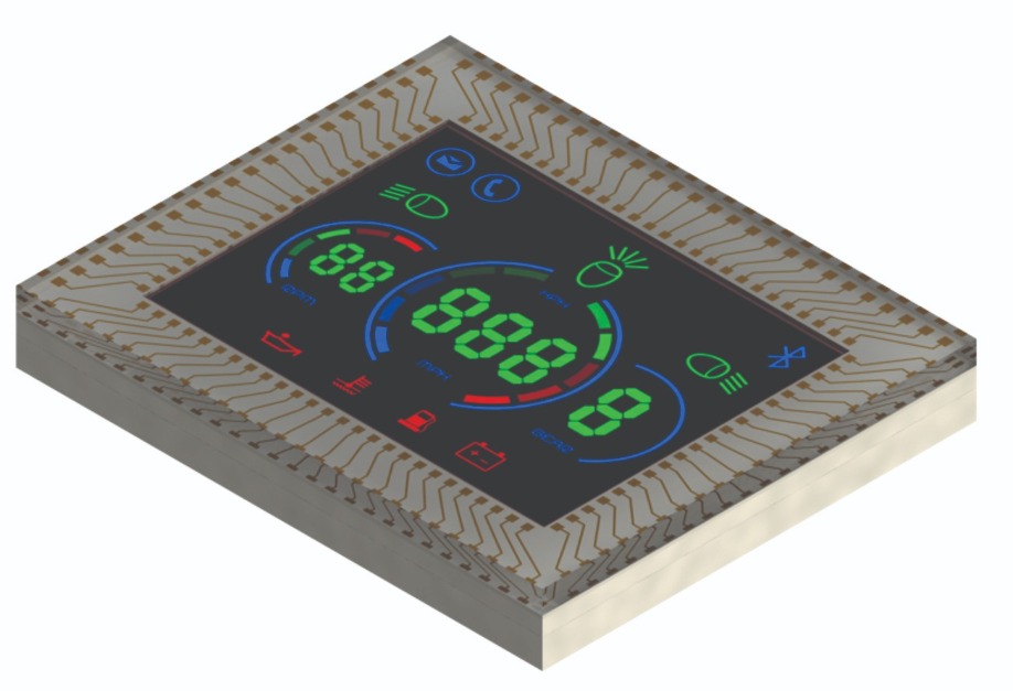
Plessey is producing direct-drive displays for many customers. They feature symbolic content, defined by etching into GaN-on-silicon epiwafers.
A very low bow is a pre-requisite for running the GaN-on-silicon epiwafers through Plessey’s silicon line, which includes wafer bonding, lithography and stepper tools. Engineers working at this site inherited a great starting position, as CamGaN’s technology focused on minimising bow. But to make microLED displays, Plessey’s engineers have had to take flatness to a new level. According to Lee, this improvement increased the yield associated with the lithography, stepper and wafer-bonding processes.Wavelength uniformity is another important criteria, due to the eye’s great sensitivity to changes in colour that can compromise the performance of a display. “Even the wavelength uniformity across the die is critical,” says Lee. By improving the process over the last year or so, wavelength uniformity across a wafer has been reduced to 10 ± 3 nm.
Display technologies also require incredibly low defect densities. Even when a particle as small as a micron comes onto the surface of a wafer during processing, it can wipe out several pixels in a display with a very small pitch. That wreaks havoc, because the eye is extremely sensitive to dead pixels.
To drive down defect levels, Plessey has taken delivery of the latest tooling that supports much lower defect levels, together with specific handling measures.
Production of displays involves chemical-mechanical polishing of GaN-on-silicon epiwafers. To reduce the chances of particle contamination, Perspex sheeting is used over the tool.
Assisted realityWith an improved production process in place, the team at Plessey is now working with companies to produce a range of assisted-reality products that contain an information display designed to work close to the eye. These are battery-driven products, operating for many, many hours, thanks to the very high efficiency of the microLEDs. Shipments are already underway, with sales expected to peak within a few years.
One example of these assisted-reality products is a scuba diving mask that incorporates a dive computer. “Another one is a sky-diving mask, so you know altitude, rate of descent and GPS, which is critical when you are sky-diving,” says Lee, who adds that assisted reality could also feature in motorbike helmets, so the driver no longer needs to look down at the dashboard; in swimming googles that provide a lap clock; and in gun scopes, offering range-finding capability and details of wind speed.
Such opportunities are very lucrative for all parties involved. For example, according to Lee, companies are coming out with products that allow them to increase the price tag for a gun scope from $500 to $1500.
All these assisted-reality displays feature symbolic content, such as arrows and numbers, rather than individually addressable pixels. In some products, one colour is used for all content, but in other designs, different colours are used for different segments.

In May 2019, Plessey unveiled a microLED display featuring an array of 1920×1080 current-driven monochrome pixels on a pitch of 8 µm. Each display requires more than two million individual electrical bonds to connect the microLED pixels to the controlling backplane.
Right now, many companies are keen to get into these markets with new products. To help them in this quest, Plessey is offering turnkey displays that emit in the red, green and blue and don’t require customisation.“The first thing they want, if they’re a larger company that has deeper pockets, is a custom version of that,” says Lee. Plessey meets this need by tailoring the colours used in the display, as well as the shapes of the emitting areas and the brightness. Turning down the latter is essential in products for night applications.
To drive further success, Plessey will launch a development kit at the upcoming Consumer Electronics Show. Known currently as Direct Drive, it features a display with dimensions below 5 mm by 5 mm, a driver that allows die to be driven at up to 2 A, a processor, and an ultra-small rechargeable battery. Symbolic content in the displays is fully customisable, using monochrome colour segments with pixel features that can be as small as 2 µm.
Production processes
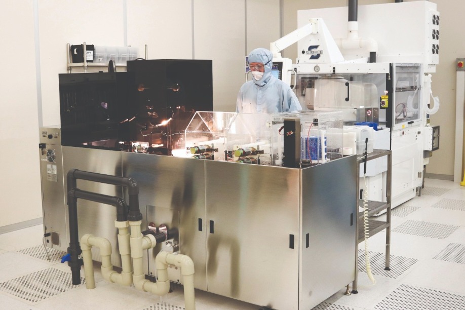
Production of these assisted-reality displays begins by loading 150 mm silicon <111> substrates into an Aixtron Crius II MOCVD reactor. To create the LED structure, a recipe with 137 steps is used to deposit a stack of GaN-based layers. The growth of GaN on silicon is challenging, as thermal and lattice mismatches between the materials can cause epiwafer bow. To prevent this from happening, the engineers use slightly thicker substrates and a complex buffer technology.
The only significant downside of the GaN-on-silicon LED architecture is that the substrate threatens to absorb the light that is emitted from the active region, dragging down efficiency. To prevent this from happening, engineers at Plessey deposit a mirror on top of the epistructure before bonding this side to a handle wafer and removing the original silicon substrate. This procedure boosts output, as light can no longer disappear into the substrate. Instead, radiation heading in this direction is reflected back into the chip, where its chances of exiting the chip are high, thanks to the texturing of the top surface.
In NOVEMBER / DECEMBER 2019 2019, Plessey revealed that it has developed a technology to form green and blue pixels on the same wafer, by growing one LED structure on top of another.
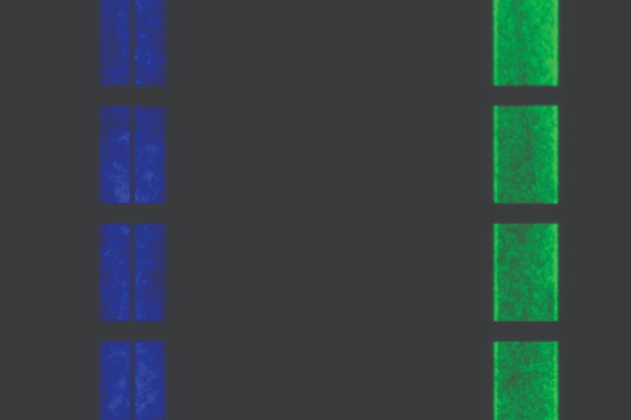
To define the symbolic content, the engineers use photolithography and etching. After this, they remove the handle wafer and apply electrical contacts to the LEDs to complete the production of these units for assisted reality displays.Plessey initially made just blue LEDs with this process. Thanks to refinement, external quantum efficiency of these 455 nm emitters is now as high as 25 percent, for a device with a 4 µm diameter. Note that when dimensions reduce, this figure falls because the periphery, where no emission takes place, becomes more significant.
One option for producing red LEDs is to crank up the indium content in the quantum wells. But efficiency plummets, due to strain-induced dislocations. So, rather than producing native red emitters, Plessey’s engineers produce sources that emit in this spectral range by coating blue LEDs with red-emitting quantum dots.
Plessey could adopt a similar approach for making its green LEDs. But it doesn’t, because there is a very low efficiency associated with the emission of green-emitting quantum dots that are pumped with a blue source. Switching to phosphors doesn’t help, as it addresses one problem while introducing another. The issue is that phosphor particles are much bigger than the pixels – and if they are ground down, this sacrifices their efficiency.
To avoid all these issues, Plessey’s engineers make native green LEDs. Their efficiency is not yet as high as that for their blue siblings – the external quantum efficiency is around 17 percent – but thanks to the far higher sensitivity of the eye in this spectral domain, they have a higher figure for cd m-2, the more important metric for displays.
Augmented reality
Manufacturing vast arrays of tiny LEDs is the critical step in the production of Plessey’s second generation of products, which will go into augmented reality headsets that provide a fully immersive experience. Lee argues that GaN-on-silicon is the ideal technology for this type of application because its efficiency lengthens battery life while enabling high brightness, so headsets can be used outdoors when the sun is out.
One of the capabilities of this technology is that it will allow the image from the smartphone to be brought to the headset. “This is a massive, growing market,” says Lee.
Many companies are working with Plessey to develop their own headset technology. Those partners incur a one-time cost to cover the expenses associated with the research, design, development and testing of a new product.
To demonstrate its prowess, Plessey recently demonstrated two displays. This May, at SID Display Week, it claimed to have produced the world’s first bonded and fully addressable GaN-on-silicon high-definition active-matrix microLED display. It has a 0.7-inch diagonal and features 1920 by 1080 pixels with dimensions of 6 µm, separated with an 8 µm pitch. The second display, unveiled this September, is even smaller – sporting a definition of 2k by 2k, it has a 2.5 µm pixel pitch.
Production of the displays begins with the growth of LED epistructures on 200 mm substrates, using an Aixtron G5+. Unlike the Crius II, this is a planetary reactor, so it offers greater uniformity and, importantly, lower defectivity levels – despite the shift from 150 mm to 200 mm wafers, there is no reduction in wavelength uniformity across the diameter.
During the processing of the wafer, which involves several lithography and etching steps, LEDs and mesas are defined in the structure. The latter contains blocking material, so that each LED is electrically and optically isolated from its neighbours.
The next step is to attach each of the processed epiwafers to a backplane. As a full high-definition display contains 1920 by 1080 pixels, 2 million individual electrical bonds are created during this process.
Plessey has found it challenging to find good suppliers of backplanes. The primary market for those companies – often design houses that outsource production – is providing backplanes to makers of liquid crystal on silicon displays. These are voltage driven, while displays for microLEDs need to be current driven.
One company addressing the need for current-driven backplanes is Jasper Display, which produces processed 200 mm wafers with its patented eSP70 silicon technology. Partnering with Jasper enabled Plessey to produce the 0.7-inch diagonal display it unveiled this May. The backplane provides 10-bit single colour control of each pixel.
More recently, Plessey announced a partnership with Compound Photonics, which will provide silicon backplanes for smart glasses. By the middle of next year, samples should be available that have a 0.26-inch diagonal full high-definition resolution, and a driver display that accepts the industry standard MIPI input.
As the display industry continues to evolve, backplane manufactures will shift to 300 mm silicon wafers and a smaller CMOS process. A reduction in the size of the CMOS process is beneficial, as it can restrict the size of the LED pixels. For example, for a 2.5 µm pixel, the maximum size for the CMOS process is 70 nm.
Plessey is well-positioned to prepare for this eventual transition, because its Crius II reactors can be used to grow 300 mm epiwafers. And when it eventually makes the move to this larger size, cost savings should follow, because the migration will trim the proportion of the wafer that is wasted.
Today, the pixelated, high-definition displays that Plessey has developed are monochrome, emitting in either the blue or the green. Obviously, that’s not what the market wants – it wants full-colour displays.
Rivals are pursuing this goal with pick and place methods. This involves producing three sets of wafers – one with red microLEDs, another with green microLEDs and a third with blue microLEDs – and transferring individual microLED chiplets onto a backplane to form RGB pixels. Efforts are focused on massively parallel techniques to speed the process. However, there are many challenges associated with positioning every microLED in the right place.
Lee and his colleague are advocating a monolithic approach, so that placement and alignment are controlled by lithography. This technology has a great track record, having enabled the tremendous scaling of the silicon transistor, in accordance with Moore’s law.
One of Plessey’s solutions is to form three separate microLED displays: one blue, another green, and a third red. To produce a colour image, the output of these three is combined with a form of prism. The image that results has a flux density of 5 W cm-2, a figure fifty times that produced by a TV. Note that an advantage of this approach over having red, green and blue pixels side-by-side is that for the same size microLED, the image has a higher resolution.
There is no doubt that the positioning of red, green and blue pixels on the same back plane is a neater solution. Plessey has started working towards this. In October it announced that it is capable of producing blue and green pixels on the same wafer, by growing one LED structure on top of another. However, adding native red microLEDs will not be easy.
Can they be caught?
Plessey is clearly in a great position right now, with a novel, powerful technology that is wooing many customers. But is there a danger that in a few years’ time, the company will be losing sales to rivals with either lower overheads, a better approach, or copycat technology?
Lee think’s not. He is certainly not worried about companies trying to flout Plessey’s intellectual property and reverse engineer the process. That’s because doing so is nigh on impossible. Even what appears to be a relatively simple task of transferring a well-established process from an Aixtron Crius II to a G5+ reactor has taken Plessey’s experienced team of engineers substantial time and effort.
Another massive barrier to competing is the cost of the infrastructure. It’s not just the investment required to purchase an Aixtron G5+. There is also the need to put together a dedicated silicon line, containing steppers, etching tools and a suite of characterisation equipment.
Last, but by no means least, Lee believes that Plessey has a first-mover advantage over any competitor that tries to replicate its technology. “We are in every deal,” says Lee.
Optimism is abounding at Plessey, and the next few years will be a very exciting time for the company. It is looking to sign more deals, make a big splash at CES 2020 and develop processes to produce even smaller pixels. In addition, it is strengthening its workforce. “We want to hire another fifty people by June 2020,” says Lee. Plessey anticipates appointing process engineers, development engineers, and those in leadership and management roles.
All these efforts promise to provide the GaN-on-silicon LED with its first ever taste of significant commercial success. While it may have appeared to have been the best option for bringing LED lighting to the masses, it’s now clear that its best chance is to drive widespread adoption of microLED displays.


