

IEDM details improvements in power electronics

Techniques for supressing degradation in SiC p-i-n diodes and IGBTs, enhancing channel mobility in SiC MOSFETs, and improving the blocking voltage and on-resistance of Ga2O3 transistors were all unveiled at the most recent IEDM meeting.
BY RICHARD STEVENSON
TURN ON THE NEWS and there’s a good chance you’ll hear a story related to climate change. Recently the focus has been on the devastating fires in Australia, but in the last few months you may also have read of accelerated ice-melting in Greenland, demolition of homes in Rwanda to protect citizens from flooding, and the breaking of global temperature records.
For those of us that see climate change as man-made, our challenge is to modify our lifestyle, so that we help to curb carbon emissions. Some of the changes that we could consider may not be to our liking, such as switching to a more plant-based diet and taking fewer flights to sunny climes. But there is one change that we will applaud: far greater deployment of more-efficient power electronics, based on devices made from alternatives to silicon.
Leading this charge is SiC. Sales of diodes and transistors made from this material are ramping fast, as the uptake of these devices branches out from their deployment in power supplies and inverters to electric vehicles, where they enable an extension to the driving range. Far behind, but with even greater promise, is gallium oxide, a material with an even wider bandgap. It will not be long before the first commercial Ga2O3 devices appear on the market, but significant sales are still some years away.
For both SiC and Ga2O3, long-term success hinges on making the devices better and better. Performance must improve, alongside reliability. To succeed, more research is needed to understand the behaviour of the diodes and transistors, and how modifications to designs impact device behaviour.
Presentations detailing progress of this nature were detailed at the latest International Electron Devices Meeting (IEDM). Held in San Francisco between 7 and 11 of December, researchers at IEDM 2019 described techniques to suppress bipolar degradation in SiC p-i-n diodes and IGBTs, improve the characteristics of the channel in SiC MOSFETs, and a Ga2O3 transistor architecture that sets a new benchmark for breakdown voltage.
Supressing bipolar degradation
Sales of SiC power devices are dominated by Schottky barrier diodes and MOSFETs. Within this commercial product portfolio there are devices designed to operate between 600 V and 3.3 kV. Higher voltages are possible, but for values of 10 kV and above, SiC p-i-n diodes and IGBTs appear to be better alternatives. However, if this pair of devices are to fulfil their potential, a condition known as bipolar degradation must be addressed. This degradation occurs when current passes through these devices and stacking faults arise, leading to an increase in forward voltage. Note that a solution to this impediment could have wider implications, as this type of affliction may also occur in body p-n diodes of SiC MOSFETs.
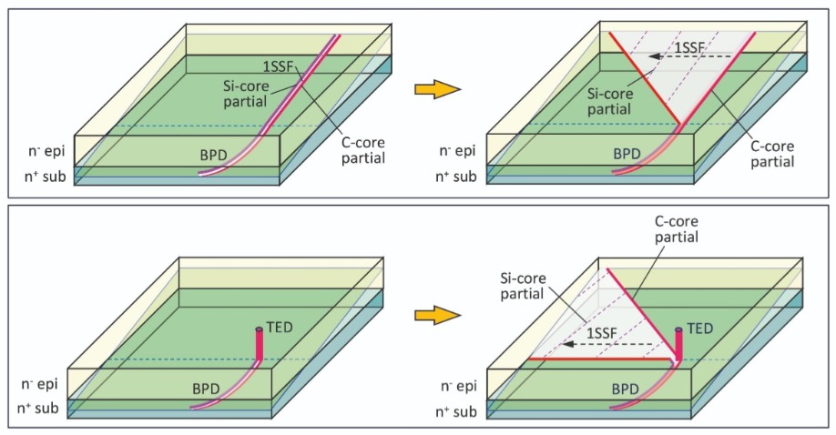
Figure 1. Basal plane dislocations (BPDs) in the substrate can propagate into the epilayer (top left), or be converted into threading edge dislocations (TEDs). Most of the BPDs in the epilayer contain a pair of partial dislocations – one with a silicon core, and the other with a carbon core – with a single Shockley stacking fault (1SSFs) between them. Once the carrier density exceeds a threshold, there is an expansion of 1SSFs from the BPDs in the epilayers to create a right-angled triangular 1SSF (top right). This expansion forms across the current pass of the device, leading to an increase in forward voltage. There can also be an expansion of 1SSFs, involving bar-shaped 1SSFs to expand from the BPD segment below the BPD-TED conversion point (bottom right). This can be caused by the injection of minority carriers into a region below the BPD-TED conversion points located near the epilayer and substrate interface, and also in substrates with a high density of BPDs.
The origin of stacking faults in bipolar devices is basal plane dislocations in the substrate. This form of imperfection comprises two partial dislocations, on either side of a narrow single Shockley stacking fault. Fortunately, during the growth of the epilayer, most of basal plane dislocations are converted into threading edge dislocations. However, a few propagate into the epilayer – most of them are in the form of screw-type basal plane dislocations.When basal plane dislocations are in the epilayers, once the carrier density exceeds a threshold, there is an expansion of single Shockley stacking faults (see Figure 1). Eventually, right-angled triangular single Shockley stacking faults are formed across the current pass of the device, leading to an increase in forward voltage.
At IEDM several approaches to combat bipolar degradation were described by Hidekazu Tsuchida from Japan’s Central Research Institute of Electric Power Industry (CRIEPI).
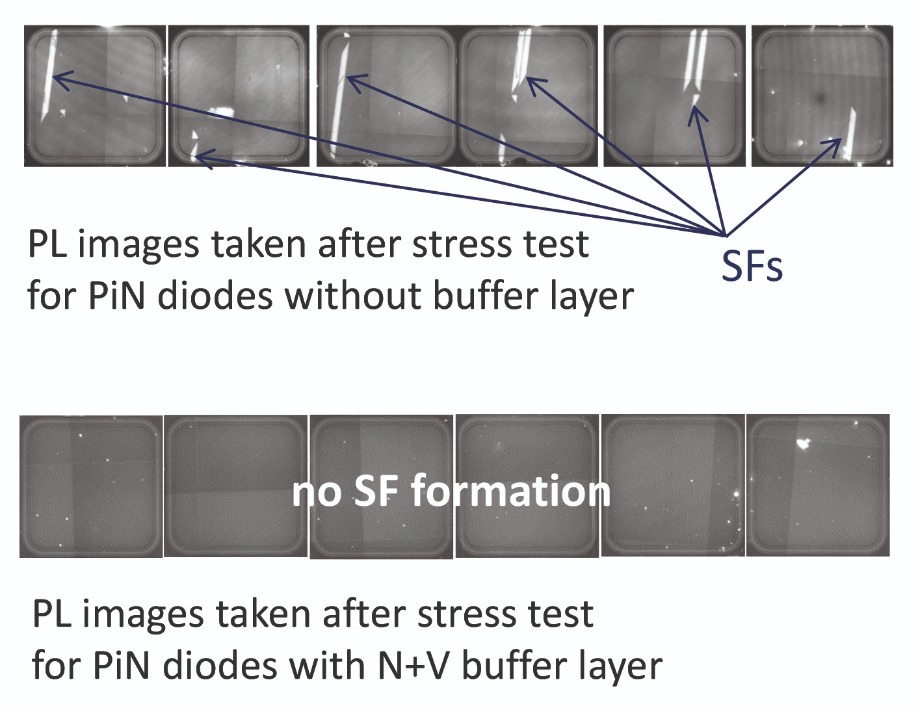
Figure 2. Photoluminescence measurements on p-i-n diodes that have been subjected to a stress test show that the addition of a buffer layer (bottom set of devices) eradicates the formation of single Shockley stacking faults.
Tsuchida, who is working with colleagues at CRIEPI, the National Institute of Advanced Industrial Science and Technology and Fuji Electric, says that it is unrealistic to expect a complete elimination of basal plane dislocations through refinements in bulk growth technology. “The average basal plane dislocation density on ‘good substrates’ has decreased a lot in the last decade. However, we still have a large variation in the quality of commercial SiC substrates.” In his opinion, the way forward is to eliminate basal plane dislocations in the epilayers by growing well-chosen heterostructures on good commercial substrates.Back in 2018, Tsuchida and co-workers reported a study involving the fabrication of SiC p-i-n diodes. This effort involved using electroluminescence to determine the threshold current associated with the expansion of single Shockley stacking faults. By measuring the charge in the drift layer during turn off, the researchers converted the current density to a hole density. This revealed that the threshold for the hole density in an n-type layer is 1-2 x 1015 cm-3.
Based on this insight, Tsuchida and co-workers argue that two criteria must be met to ensure the suppression of bipolar degradation. They are the elimination of basal plane dislocations from the region where minority carriers are injected, and the reduction in the minority carrier density to a level below threshold in the region where basal plane dislocations exist.
According to Tsuchida, both these requirements are needed because even if basal plane dislocations in the substrate are perfectly converted to threading edge dislocations at the interface between the epilayer and the substrate, minority carriers are still injected into the substrate. Here, the danger is that the density of these carriers exceeds the local threshold, triggering conversion of the basal plane dislocations in the substrate into stacking faults.
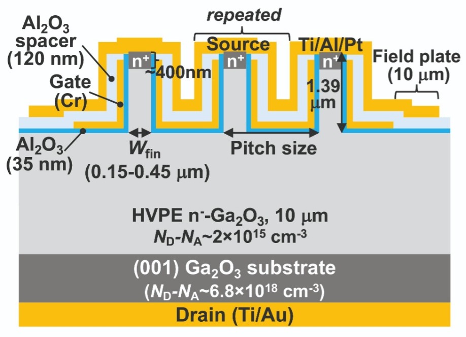
Figure 3. Ga2O3 transistors with multiple fins have broken the record for the blocking voltage for this class of transistor. A portfolio of devices has been produced, with fin channel widths ranging from 0.15 µm to 0.45 µm, and pitch sizes from 1.2 µm to 2 µm.
The solution, according to Tsuchida, is to insert a buffer layer with a short carrier lifetime between the substrate and drift layer. This addition reduces the injection of minority carriers into the substrate region.Initially, the team turned to nitrogen doping to reduce the carrier lifetime in the buffer. However, when the nitrogen concentration exceeded 1-2 x 1019 cm-3, this introduced an imperfection known as a double Shockley stacking fault. Keeping the nitrogen concentration low enough to avoid this shortened the carrier lifetime to around 40 ns.
To further reduce this lifetime, Tsuchida and co-workers have recently switched to doping with vanadium, a deeper dopant. When present at a concentration of just 7 x 1014 cm-3, room-temperature carrier lifetime is shortened to just 13 ns.
The benefit of vanadium doping has been assessed by comparing two sets of SiC p-i-n diodes. Controls features a 10 µm-thick, nitrogen-doped drift layer grown on an n-type substrate, and modified variants have an additional buffer, doped with vanadium and nitrogen, inserted between the substrate and drift layer.
To evaluate the impact of the buffer, measurements were made on 16 controls and 16 variants. Initial forward voltages, recorded at a 18 A drive current, were compared with values after one stress test and then another. The first involved driving diodes at 300 A cm-2 for an hour, and for the second, devices were run at 600 A cm-2 for an hour. Analysis of the results showed that the buffer layer leads to a substantial reduction in variation of forward voltage after operation.
Further insight into the difference between standard devices and those with a doped buffer has come from photoluminescence measurements. This optical technique exposed single Shockley stacking faults in the conventional diode, and the absence of these faults in the modified design (see Figure 2).
Buffer layers may also benefit SiC IGBTs. This type of device would require a p-type buffer layer with a short carrier lifetime. Aluminium, which forms a shallow acceptor, is a candidate for doping, as increases in its concentration reduce carrier lifetime. Tsuchida and co-workers suggest that this might be combined with boron, which greatly shortens carrier lifetime.
One of the goals for the team is to map, with precision, the locations across a wafer where basal plane dislocations are converted into threading edge dislocations. Such a study promises to enable a more detailed, quantitative understanding of the expansion of single Shockley stacking faults, and could also aid the development of drift and buffer layers that improve the performance of bipolar devices.
Another target for the researchers is the development of a fast growth technique for making 4H SiC that will trim the density of basal plane dislocations and threading dislocations. The team have already made much progress, realising a growth rate of 3 µm/hour. “[That’s] about ten times higher than a typical PVT growth,” says Tsuchida.
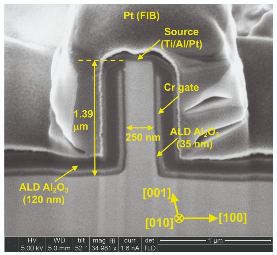
Figure 4. A scanning electron microscopy image of the fins in the Ga2O3 transistors highlight the near-vertical sidewall profile produced by dry etching.
MOSFET modificationsThe introduction of a new dopant is also behind the improvements made to the performance of SiC MOSFETs. This success, realised by a team from Mitsubishi, involved the introduction of oxygen doping. It led to a significant reduction in channel resistance and an increase in the threshold voltage.
Both of these attributes are highly desired by the designers of power electric systems. Reducing resistance cuts energy losses, and a higher threshold voltage makes it easier to control the system.
Normally these improvements are realised by nitridation. However, if the threshold voltage exceeds 3 V, this comes at the expense of a hike in channel resistance.
The team from Mitsubishi have previously addressed this weakness by switching to sulphur. And at IEDM they revealed the results of using another alterative, oxygen, which is a far deeper donor. Spokesman for the team, Munetaka Noguchi, claims that there are no downsides to the use of deep donors. He arrived at this conclusion after considering the results of pulsed measurements that enable an estimate of threshold voltage stability.
Noguchi and co-workers have produced vertical and lateral SiC MOSFETs with oxygen doping. For commercial sales, vertical MOSFETs are preferred. “We used lateral MOSFETs as a test structure to evaluate channel performance,” explains Noguchi.
Ion implantation provided a relatively high concentration of oxygen near the channel. Note that such a high concentration is not possible with simple thermal oxidation. Following thermal activation of oxygen, the team formed the gate oxide with thermal oxidation and nitridation in dilute nitrogen oxide.
Measurements of the capacitance of the MOS capacitors in the lateral MOSFETs revealed that at elevated temperatures the introduction of oxygen increases capacitance in the depletion region. This work also revealed that oxygen acts as a donor, rather than an acceptor-like trap.
Additional benefits of the introduction of oxygen in lateral SiC MOSFETs include a 46 percent reduction in channel resistance, realised for a threshold voltage of 3.9 V.
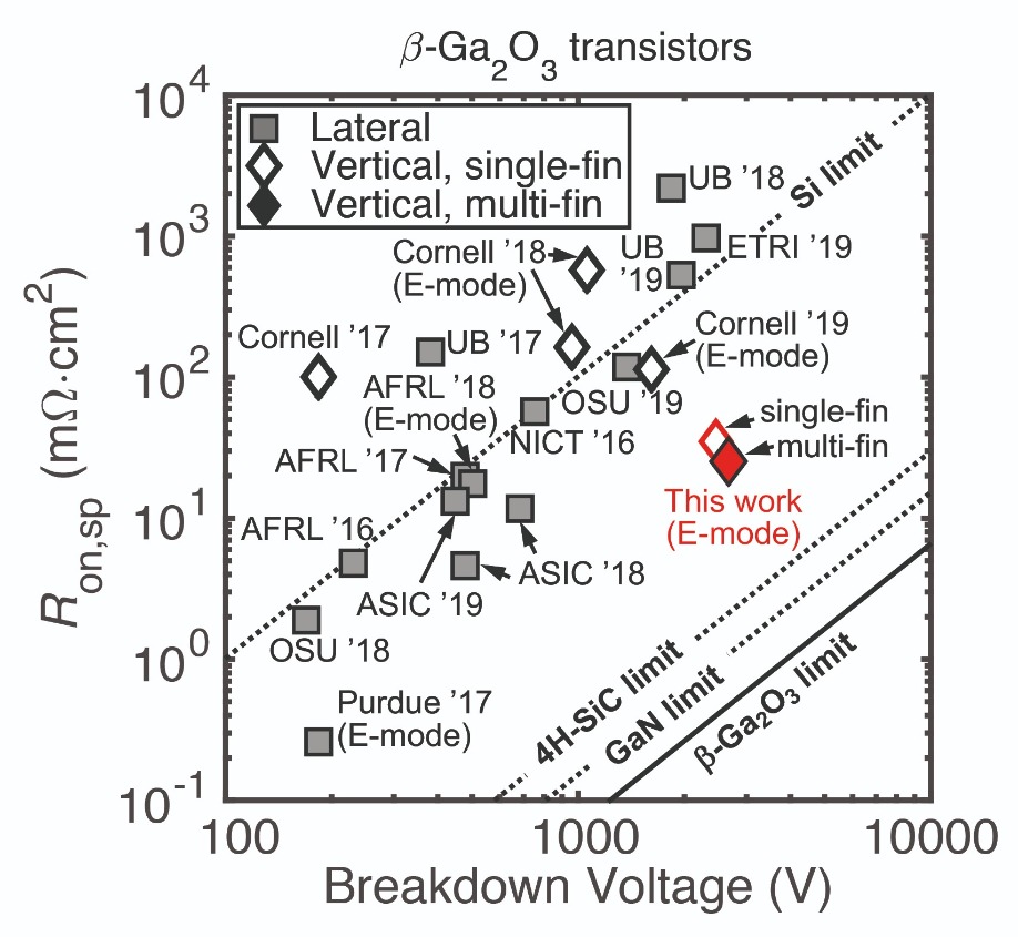
Figure 5. Multi-fin Ga2O3 transistors produce by a partnership between researchers at Cornell University and Hosei University have broken the record for blocking voltage for this class of device. Note that the on-resistance is normalised using an effective conduction width of about 10 mm, as normalising this resistance to the source contact area would grossly over-estimate the figure of merit.
Vertical MOSFETs with oxygen doping also produce encouraging results. Devices with a threshold voltage of 4.5 V have a 32 percent reduction in the total on-resistance.When using any deep level donor, there is an increase in the threshold voltage drift at elevated temperatures. “However, the magnitude is suppressed in the oxygen doped sample,” says Noguchi. Compared to sulphur, this shift is almost halved.
Another benefit of using oxygen rather than sulphur is that it produces a smaller shift in negative bias temperature instability. This indicates that the reliability of the gate is better – it is, in fact, comparable to that in a conventional device.
Noguchi and co-workers will continue to investigate the impact of deep level donors on the electrical characteristics of the MOSFET. In particular, they will consider its ruggedness as a power switching device.
Another option for decreasing the resistance of a SiC MOSFET is to use a trench architecture. This design also allows a smaller cell pitch, leading to an increase in channel width.
However, the trench MOSFETs that have been fabricated on commercial SiC (0001) substrates are failing to fulfil their promise. The field-effect channel mobility is lower than that expected for planar MOSFETs, for reason that are not clear.
To shed light on this matter, a team from Toyota Central R&D Labs has tried to determine the mobility in the channel. To extract an accurate channel resistance, they remove parasitic series resistance from their calculations.
According to the researchers, the key to calculating the field-effect channel mobility is to determine the threshold voltage. Due to the high density of charge traps at the interfaces of SiO2 and SiC, there are inaccuracies associated with calculations of threshold voltage that are based on linear extraction. To avoid this, the team determines the threshold voltage by drawing on values of the ideal threshold voltage and experimental measurements of the relationship between the drain current and the gate voltage.
The first step towards this involved growing n-type and p-type epilayers of SiC on a heavily doped n-type SiC substrate. After adding source and drain regions, the researchers fabricated a trench gate. Following trench etching, they used three different forms of high-temperature annealing to produce different surface morphologies in the trench walls. To complete the fabrication of the structure, they added a 75 nm-thick layer of SiO2, followed by nitridation of the device in diluted nitrogen oxide.
Plotting the drain current as a function of gate voltage at a range of temperatures enabled the team to calculate the density of fixed charges and the distribution of interface states. From these values, the researchers concluded that the interface states contribute to Coulomb scattering.
To relate the level of scattering to the quality of the channel, the team scrutinised the surface morphology of the trench sidewalls with atomic force microscopy. This revealed a significant difference in the roughness of the three samples. By combining this finding with the electrical measurements, they deduced that Coulomb scattering is suppressed when the trench sidewalls are flat enough to form atomic steps and terraces. In this case channel mobility is higher, due to a decrease in the distribution of interface states that arises from dangling bonds at the edge of the step region.
Record-breaking voltages
Helping to improve the performance of Ga2O3 transistors is a partnership between researchers at Cornell University and Hosei University. This team has broken the record for blocking voltage with a vertical transistor that can withstand 2.66 kV. This raises the bar from 2.32 kV, a figure obtained with a lateral variant.
Team spokesman Wenshen Li from Cornell University says that one of the merits of the vertical architecture, which leads to vertical current flow, is a more efficient use of the device footprint. “[Devices] typically have a smaller area, especially under high current ratings.”
By using a sub-micron fin-channel structure for the device architecture (see Figure 3), Li and co-workers avoid the need for p-doping. That’s a significant advantage as p-doping in Ga2O3 is impaired by: deep acceptor levels that hamper the thermal activation of these carriers; a very flat valence band, which leads to a high effective mass for holes and impairs conductivity; and self-trapping of holes.
One of the reasons why Ga2O3 transistors are failing to fulfil their potential is that the channel mobility is far lower than it is in the bulk, due to etch damage and sidewall depletion. Effective channel mobility is typically just 30 cm2 V-1 s-1, compared to values of up to 200 cm2 V-1 s-1 for bulk material.
To address this, Li and co-workers use a post-deposition annealing step during the production of their transistors. Some of these devices contain several fins, enabling unambiguous evaluation of the specific on-resistance – it breaks new ground for Ga2O3 transistors.
Fabrication of the team’s devices began by loading an n-type Ga2O3 substrate into a HVPE chamber and depositing a 10 µm-thick, lightly doped n-type drift layer. Silicon implantation and subsequent activation at 1000 °C created a heavily doped n-type top layer that provided an ohmic contact. Electron-beam lithography defined the fins (see Figure 4), which were formed by dry etching.
After treatment with HF to remove plasma damage, the team added a Ti/Au drain contact and a gate contact, comprising a 35 nm-thick Al2O3 gate dielectric created by atomic layer deposition and a 50 nm-thick layer of chromium, deposited by sputtering.
During the formation of the source electrode of Ti/Al/Pt by sputtering, Li and co-workers simultaneously created a source-connected field plate. This refinement to the design provided a significant improvement to edge termination, and is behind the increase in breakdown voltage.
“However, we found that the breakdown voltage is still limited by the edge termination, indicating that the source-connected field plate is not an optimal design,” admits Li.
The team have used electrical measurements to evaluate the benefit of post-deposition annealing. It leads to a significant increase in current density, an improved source contact resistance, and a reduction in interface trapped charges, leading to a lowering of the sidewall depletion in the fin channels.
Using simulations and fits to experimental data, channel mobility in single-fin devices is found to be around 130 cm2 V-1 s-1. This figure drops to just 40 cm2 V-1 s-1 in multi-fin devices, due to rougher sidewalls that result from plasma loading effects during the dry-etching step. “By tweaking the plasma condition during the dry etching for a more anisotropic etch, the roughness can be reduced,” say Li.
The multi-fin device outperforms its single-fin variant in blocking voltage, realising a value of 2.655 kV, compared with 2.46 kV. Additional measurements on the multi-fin transistor reveal an on-off ratio in excess of 108; a threshold voltage of 1.8 V at 0.1 mA cm-2; and a specific on-resistance of 23.2 mΩcm2, based on pulsed-measurements that are expected to reduce self-heating and charge trapping (see Figure 5 for benchmarking of the single-fin and multi-fin devices) .
Plans for further work include optimising the dry etching process, in order to improve channel mobility in multi-fin channel devices, and developing better edge termination designs for improved breakdown behaviour. Li says that additional goals are to undertake thermal characterisation of their devices, and the testing and analysis of dynamic behaviours.
The presentations at IEDM by Li on Ga2O3 transistors, and by other speakers on SiC devices, show that power electronic devices are getting better. That bodes well for the future, where greater deployment of more efficient power electronics is set to play its part in global efforts to tackle climate change.


