Toward high resolution multi-colour imaging

Wafer bonding opens the door to the fabrication of multi-colour, high-resolution imagers.
BY Sanghyeon Kim, Dae-Myeong Geum FROM Korea Advanced Institute of Science and Technology, Won Jun Choi FROM Korea Institute of Science and Technology AND Euijoon Yoon FROM Seoul National University
Deployment of photodetectors is on the rise. Those operating in the visible are now a key feature in smartphones, and variants detecting in the infrared are being used in surveillance and the development of autonomous cars.
Product designers are selecting photodetectors that operate within a particular spectral domain to retrieve specific information. Detectors of visible light provide visual information our eye can see. Meanwhile, those operating in the infrared, where our eyes cannot see, offer details of the height of an object, or some chemical information – this is crucial in many applications.
Recently, there has been great interest in simultaneous detection across different spectral regions. The development of multi-wavelength photodetectors promises to revolutionise sensing and imaging applications, such as gas detection, medical diagnostics, industrial surveillance and time-of-flight sensors. By constructing overlapping images at different wavelengths, it is possible to generate more informative, more accurate, and more creative information.
Downsides of multi-colour photodetectors, including those that have been recently reported and those that have been commercialised, are bulkiness and use that is restricted to the lab. The only approach to making them that has been commercialised is packaging-based integration. This involves the positioning, in a vertical plane, of a silicon photodetector for the visible and an InGaAs variant for the infrared. With this geometry, when light is separated by a diffraction grating, the differing spectral domains are directed at appropriate detectors (see Figure 1). However, adopting this approach hampers the production of compact, high-resolution imaging devices – the detectors are relatively large, and alignment accuracy is limited by the mechanical alignment between the silicon and InGaAs photodetectors.
One alternative is epitaxy-based integration. With this approach, multi-colour photodetectors are formed by growing multiple active regions. This addresses the issue of bulkiness, but due to lattice mismatches between the different sections, the photodetector is impaired by high power consumption and degraded material quality.
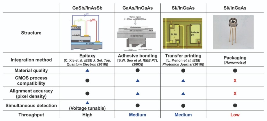
Figure 1. There are many different methods to fabricate multi-colour photodetectors.
Additional alternatives involve transfer printing and adhesive bonding. But they are compromised by limited vertical and horizontal alignment, as well as a low pixel density.A far better way forward, pursued by our partnership between researchers at Korea Advanced Institute of Science and Technology (KAIST), the Korea Institute of Science and Technology (KIST), and Seoul National University (SNU), is the monolithic integration of visible and infrared photodetectors. Employing wafer bonding and epitaxial lift-off techniques, this enables high-resolution, multi-colour imaging.
Multi-colour capabilities
At the heart of our fabrication process is the wafer bonding technique. This low-temperature, low defective process allows us to unite different materials without having to address concerns relating to lattice mismatch (see Figure 2).
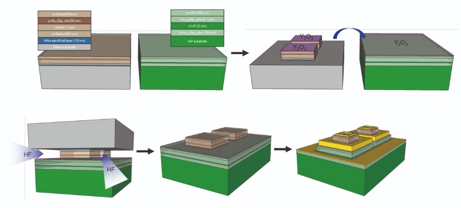
Figure 2. Process flow for multi-colour photodetectors made from GaAs and InGaAs using wafer bonding and an epitaxial lift-off process.
We select GaAs as the light-absorbing material for visible wavelengths, and use InGaAs for infrared detection. Both detectors are formed by epitaxy: GaAs substrates are used for the growth of visible detectors, and those made from InP are used to make detectors operating in the infrared. To separate the GaAs photodetector from its native substrate after the wafer bonding step, we insert a sacrificial AlAs layer between the device and its substrate.After growing both types of epiwafer, we deposit a layer of Y2O3 on both of them. This oxide is inserted because it is a suitable bonding material, and it has good material stability in the presence of HF, an acid used in the epitaxial lift-off process. After this, we undertake mesa isolation to enhance the speed of the epitaxial lift-off process (this process is detailed in our previous article, published in the June 2017 edition of Compound Semiconductor magazine). The two samples are then bonded together, and the resultant entity dipped in HF acid to separate the GaAs donor substrate from the stack of materials that contains the GaAs photodector, the InGaAs photodetector and the InP substrate. Finally, using standard semiconductor process technology, we undertake metal formation and mesa isolation.
Note that with our approach we form pixels after wafer bonding, using photolithography and etching. This allows us to use a small pitch, and create a high-resolution photodetector (see Figure 3 for microscopic top-view images of fabricated pixels). One of the merits of the multiple pixel array, formed by vertically stacking two photodetectors, is that it delivers twice the resolution of a conventional approach.
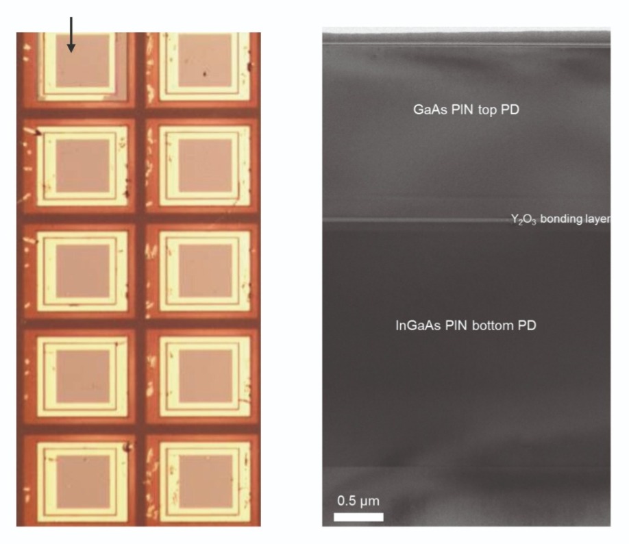
Figure 3. Photographic top-view image and cross-sectional transmission electron microscopy images of the fabricated stacked GaAs visible photodetector and infrared InGaAs photodetectors. These images reveal the good bonding, and also the high material quality after the bonding.
Scrutinising our structures with cross-sectional transmission electron microscopy highlights the good bonding quality and material quality between the layers made from GaAs, and those made from InGaAs. The quality of our stacked material is very high – it is nearly as good as the as-grown sample – and it leads to good electrical and optical performance for the fabricated photodetectors.Optical performance
We have broken new ground by demonstrating vertically well-aligned, multi-colour photodetectors formed from typical semiconductor processes. They detect from 400 nm to 1650 nm, a range so broad that it cannot be realised with a single absorbing material (see Figure 4). Measurements of photoresponsivity show similar levels for GaAs and InGaAs photodetectors, highlighting the excellent match between this pair of materials.
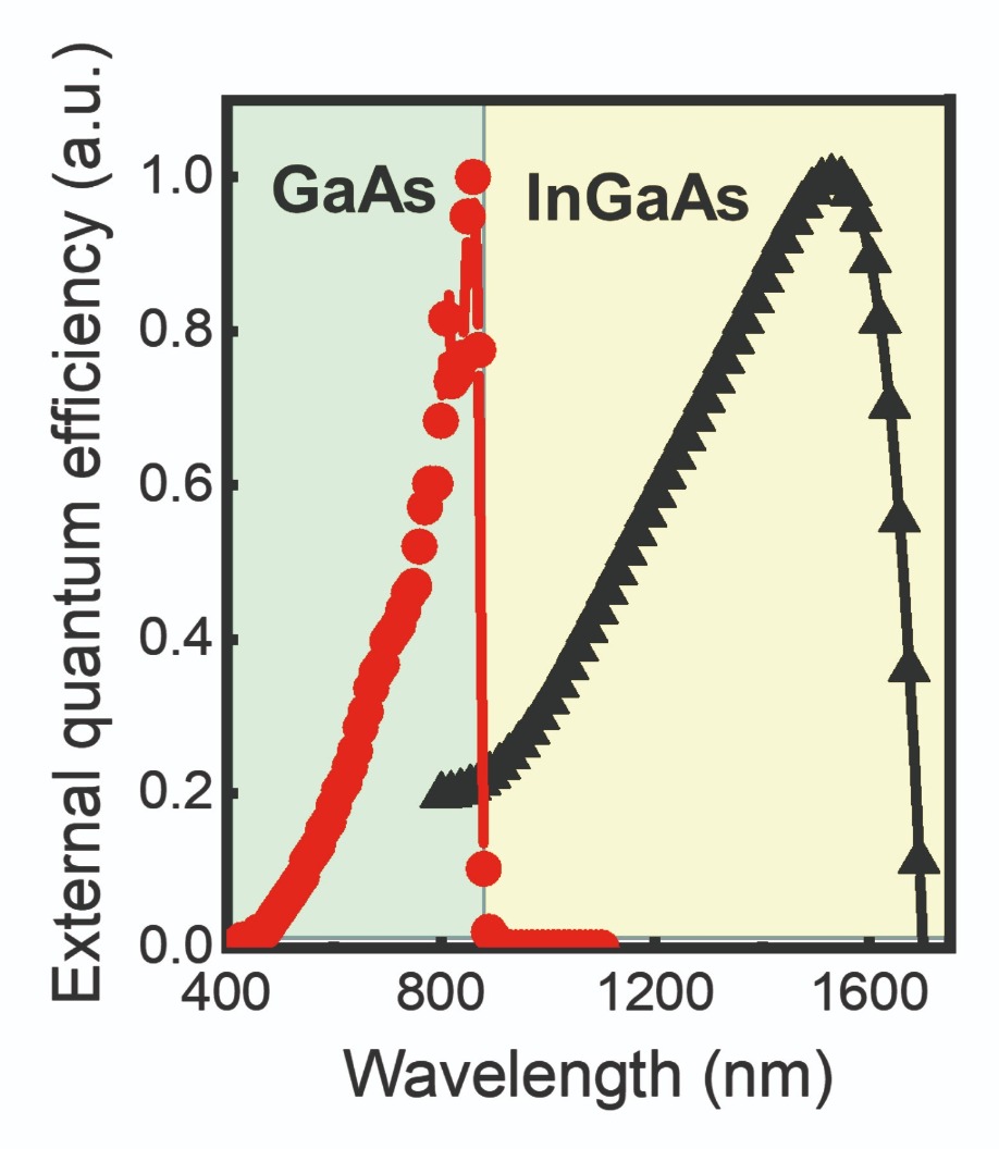
Figure 4. The external quantum efficiency of the fabricated multi-colour photodetectors, highlighting very broad band absorption from 400 nm to 1650 nm.
The insulating Y2O3 film between the two photodetectors enables independent operation. Visible light is absorbed in the top GaAs photodetector, while infrared light passes through it and is absorbed in the bottom InGaAs photodetector. Simultaneous measurements from a single device, shown in Figure 5, demonstrate that we have made a promising step towards the fabrication of a high-resolution, multi-colour imager, formed from high-quality III-V light absorbing layers.Our next goal, the fabrication of imagers, requires the hybrid integration of photodetectors with readout integrated circuits (ROICs).
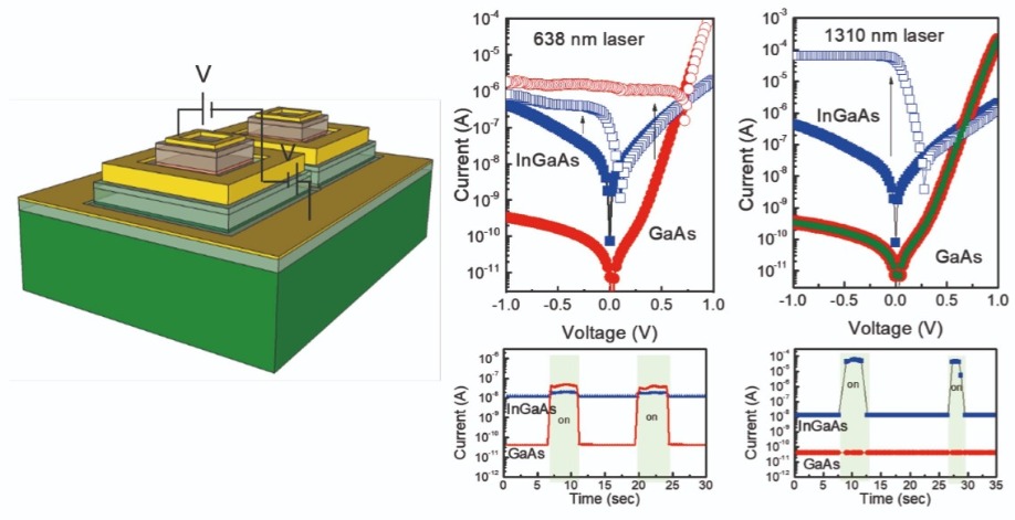
Figure 5. An illustration of the stacked multi-colour photodetectors, and plots of the photoresponse of photodetectors to visible and infrared excitation
Often the integration is accomplished with indium bump bonding. This is quite a complicated process that includes thick indium deposition, reflow, flip chip bonding, and epoxy underfill. What’s more, it involves mechanical alignment between III-V imagers and ROICs, limiting pixel resolution.We are pursuing a slightly different approach to integrating multi-colour imagers on ROICs. After forming the ROICs, our intention is to bond the first absorbing materials and then the second absorbing materials, processing them using mesa formation, metallization and so on. With this approach, we can draw on the benefits of lithography, which delivers the very precise alignment needed to form high resolution pixels.
Our efforts have enabled us to make great progress towards the fabrication of multi-colour photodetectors. Combining light absorbing layers of GaAs and InGaAs by wafer bonding offers many advantages over conventional integration methods, including good material quality, CMOS process compatibility, precise alignment accuracy between pixels, and simultaneous broad band detection.
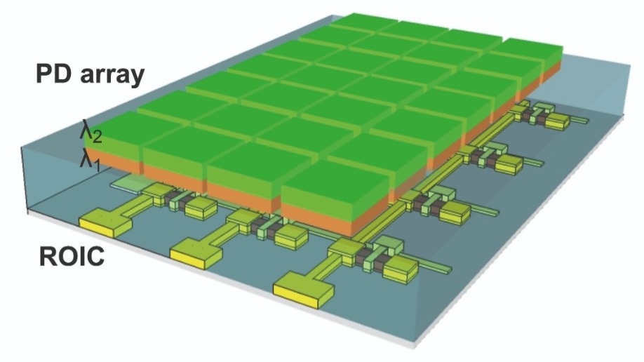
Figure 6. A potential integration method for making multi-colour photodetectors on ROICs.
When we realise our next milestone, the fabrication of high resolution, multi-colour imagers, our success will open up many new markets. That’s because there is a tremendous opportunity to develop many promising applications enabled by our technology, such as artificial vision sensors with coloured image recognition functions.D. -M. Geum et al., “Monolithic integration of GaAs//InGaAs photodetectors for multicolor detection”, VLSI symposia, p. T248 (2019)
S. Kim et al. Appl. Phys. Lett. 110 153505 (2017)


