
The little-known path to high efficiency light emitters
Designers of blue and green LEDs avoid wide quantum wells, arguing that they impair efficiency, due to built-in fields that pull electrons and holes apart. But that’s an incomplete picture: turn to excited states and high radiative efficiencies are realised over a broad spectral range.
BY GREG MUZIOL FROM THE INSTITUTEOF HIGH PRESSURE PHYSICS, Polish Academy of Sciences
LEDs are everywhere. They are lighting our homes, offices and neighbourhoods; they are backlighting our TVs, tablets and smartphones; and they are in our torches, headlights and many of our gadgets. Sales of these devices now net billions and billions of dollars every year, with success driven by the high internal quantum efficiency of these emitters – in state-of-the-art blue and violet LEDs, the internal quantum efficiency peaks at more than 90 percent.
However, the internal quantum efficiency is not always that high, due to the primary loss mechanism varying with drive current. When LEDs are driven in the low carrier regime, efficiency is limited by non-radiative recombination at defects, through the Shockley-Read-Hall process. Reducing the density of defects by optimising material drives down the losses via this mechanism, leading to a high internal quantum efficiency.
As the current through the LED is cranked up towards the ideal operating range, there is an increase in non-radiative recombination caused by the Auger process. These losses are an unavoidable property of the material, and are surprisingly high in III-nitrides. What’s particularly concerning is that when Auger recombination is the primary loss mechanism, the higher the current, the greater the loss, leading to a steady decline in internal quantum efficiency. Due to this malady, commonly known as droop, there is a constraint on the operating conditions for the LED – it must be driven at a low current density to ensure a high efficiency, and this restriction means that for a given output, high efficiency is realised with a chip with a large footprint.
At first glance, one straightforward solution to combatting droop is to increase the width of the InGaN active region, as this reduces the carrier density for a given current. Adopting this approach should shift the onset of droop to a higher drive current, enabling a reduction in the footprint of the device. However, this solution has its downsides, as InGaN has a giant piezoelectric constant. This creates a high built-in polarization in the quantum well that is known to pull apart electron and hole wavefunctions, reducing the likelihood of radiative recombination. What’s more, InGaN has a large lattice mismatch to GaN, hampering the growth of thick quantum wells.
As well as droop, there is another bottleneck to realising a high internal quantum efficiency in LEDs. As the indium content in the InGaN wells increases to propel emission from the blue to the green and yellow, efficiency falls. Turning to another material is not an option, as only nitrides can span these wavelengths.
There are many reasons behind the decline in the efficiency of nitride LEDs at longer wavelengths. Material quality degrades as indium content increases, leading to more defects, which drag down efficiency; the built-in field is higher, making radiative recombination less likely; and there is a hike in non-radiative Auger recombination. The latter two are responsible for the higher droop in longer-wavelength devices.
Fortunately there is a simple, yet overlooked, solution to addressing both of these bottlenecks, that has been proposed recently by our team at the Institute of High Pressure Physics of the Polish Academy of Sciences. Our idea, which will come as a shock to many in the nitride community, is to use wide wells, despite their drawbacks. Why, given all the issues outlined above? Because for exited states, the overlap of the electron and hole wavefunctions is high in wide wells. This is particularly welcome for green and yellow emitters, where the increase in efficiency is even more pronounced.
Bandstructure benefits
To understand why our solution is beneficial, one needs to see how the bandstructure evolves as the wells get thicker. We have gained an insight into this by calculating the band structure of thin and thick wells – they are 2.6 nm and 10.4 nm wide – with and without excitation (see Figure 1). Whether this excitation is optical or electrical does not change the general picture.
For the thin well, excitation increases the wavefunction overlap from 0.19 to 0.39, due to screening of the polarization. Although this is a substantial increase, it does not change the qualitative behaviour of the transition.
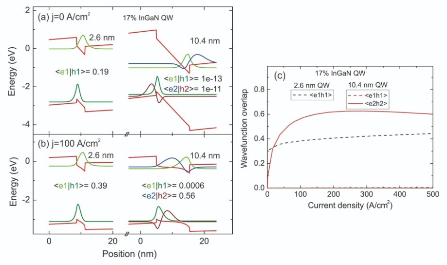
Figure 1. Calculated band structure of a thin (2.6 nm) and a wide (10.4 nm) In0.17Ga0.83N quantum well (a) without and (b) with excitation. (c) Dependence of wavefunction overlap on current density. Above a current density of 16 A/cm2 the
To our knowledge, this is the first demonstration of a quantum well system that has a zero-probability transition between the ground states, but an extremely high one through the excited states. This situation, caused by the huge difference between the overlaps of the ground and the excited states, results from substantial differences in localization. Despite the screening of the piezoelectric field, ground states are still localized in the triangular part of the quantum well (see Figure 1(b)). In stark contrast, the excited states, which have higher energies, fill the entire width of the well. These excited states can be thought of as existing in an almost rectangular quantum well, with small perturbations at the interfaces. In other words, the overlap is almost equal to unity, just like it is in a quantum mechanics textbooks detailing the solutions to a particle in a finite square well.
Testing the theory
Are these findings borne out in practice? To find out, we have produced a portfolio of samples that have In0.17Ga0.83N wells with various widths (the heterostructures are shown in the inset of Figure 2(a)). At high excitation levels that produce excited states, the photoluminescence intensity increases, as predicted (see Figure 2 (a)).
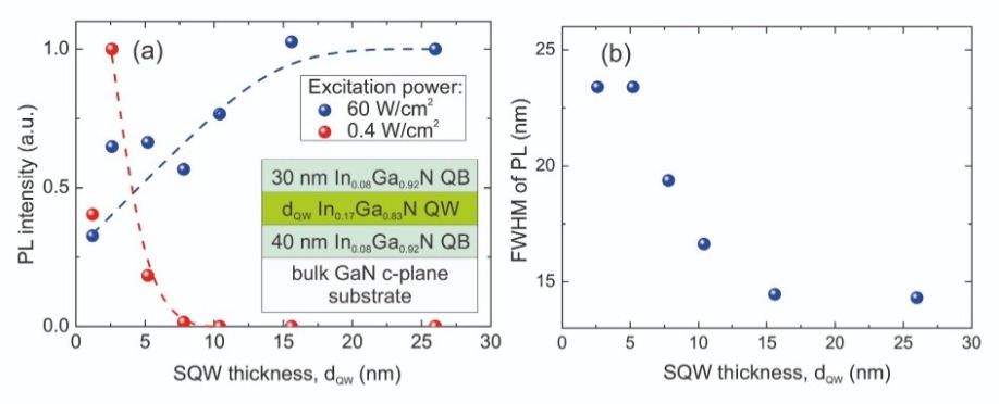
Figure 2. (a) Dependence of photoluminescence intensity of the quantum well thickness for two excitation powers. The inset shows the structure of samples. (b) Dependence of the full-width at half-maximum of photoluminescence measured at an excitation power of 60 W/cm2.
At a lower excitation level the opposite occurs, with a thicker well producing a weaker photoluminescence signal. This is to be expected, if one adds a small carrier loss mechanism to the model. For wider wells, carriers are unlikely to initially recombine, because a high carrier concentration in the ground state is needed to screen the piezoelectric sheet charges. As the carriers accumulate in the ground state, some will be thermionically emitted to the surrounding barriers. Due to this loss, the carrier density is never high enough, in the low excitation regime, to enable the screening required for a strong photoluminescence signal.It is intriguing to know at what point the carrier and the current densities are high enough to fill the excited states and take advantage of their high oscillator strength. At both interfaces of an In0.17Ga0.83N quantum well, sheet charges induced by strain are equal to 1.7x1013 cm-2. Screening these charges requires the introduction of a matching number of electrons and holes in the quantum well. For this to happen, the corresponding carrier density should be equal to 5×1019 cm-3. This is a very high number. To put it into perspective, such a high carrier densities is only seen at very high current densities, such as those found in laser diodes at threshold. But this is true only in the case of thin quantum wells.
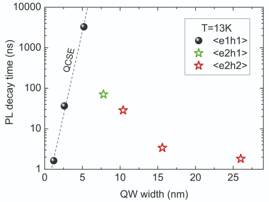
Figure 3. Dependence of photoluminescence decay time on the quantum well width. The legend gives our interpretation of the nature of the observed transition. The dashed line is a guide to the eye, showing the behaviour predicted by a drop of wavefunction overlap with quantum well thickness.
To make a meaningful assessment it is critical to calculate the LED bandstructure, as this reveals the interplay between the accumulation and the loss of the carriers. Counterintuitively, in wide wells, screening of the piezoelectric field occurs at relatively low current densities (see Figure 1(c)), which are comparable to the operating regime of standard LEDs. This implies that LEDs with wide wells can benefit from the decreased carrier density and the higher onset for droop – and can be driven harder, to deliver the equivalent output for a smaller footprint without compromising efficiency.Another benefit of a wider well is that it offers a greater robustness to variations in the quality of the quantum well interfaces. In thin wells, if there are variations in width by just a monolayer, this has a profound impact on the emission profile, including an increase in the full-width at half-maximum. This is a big issue, because unwanted broadening is detrimental to laser diodes, which require as narrow an optical gain as possible. Increasing the thickness of the well has a dramatic impact on the profile of the width of the emission peak. Replacing a well that’s just 2.6 nm-thick with one as wide as 15 nm can narrow the full width at half-maximum for the photoluminescence peak from 23 nm to just 14 nm (see Figure 2(b)).
Measurements of carrier dynamics provide additional proof of the qualitative difference between thin and thick wells. Just a small increase in the thickness of thin wells results in a substantial increase in the decay time of the photoluminescence signal, with values as high as 3 µs observed in 5.2 nm-thick wells. Such a significant increase in photoluminescence decay time is a hallmark of a system with a high dependence of oscillator strength on the thickness of the quantum well (see the region marked with a dashed line in Figure 3). For the 5.2 nm-thick well, the wavefunction overlap for the ground state is calculated to be only 0.0006. When the thickness of the well is increased much beyond this, the decay time starts to drop, with the active region moving into a regime where excited states start to play a major role in recombination.
At longer wavelengths, where the green gap is found, wider quantum wells start to fulfil their true potential. For green-emitting In0.3Ga0.7N wells with a 10.4 nm width, wavefunction overlap can hit 0.63, a value associated with the first excited state (see Figure 4 (a)). This surprisingly high value reveals that the oscillator strength is far higher than that for thin quantum wells.
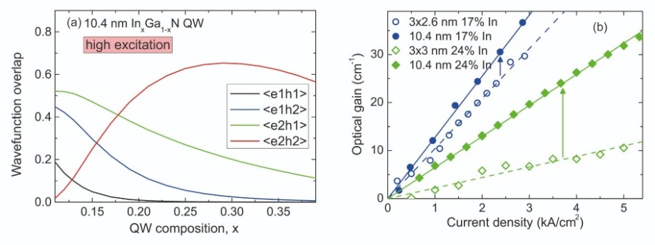
Figure 4. (a) Calculated dependence of wavefunction overlap on quantum well composition. (b) Measured optical gain of four laser diodes with different active region designs given in the legend. Solid and dashed lines are used to extract the differential gain. The arrows indicate the increment realised due to the use of the wide quantum well.
To understand why this is the case, one must note that the high oscillator strength comes from the high value of the piezoelectric polarization. Increase this and there is a hike in the sheet charges generated at the interfaces, leading to a more rectangular profile for the quantum well after screening. The upshot is that the excited states have a higher wavefunction overlap.Making lasers
Our efforts at highlighting the benefits of wider wells have included the fabrication of a range of laser diodes, operating in the blue and cyan, at wavelengths of 450 nm and 490 nm, respectively. This portfolio includes lasers with three quantum wells with thicknesses ranging from 2.6 nm to 3 nm, and devices with a single, 10.4 nm-thick quantum well.
Using the Hakki-Paoli method we have measured the optical gain in these devices. This reveals a linear increase with current density (see Figure 4(b)). When the optical gain increases rapidly with current density, this is indicative of either an increase in the efficiency of the quantum well or an increase in the optical confinement factor. Both of these are enhanced with wider wells in the active region. In the case of blue lasers, for the three 2.6 nm-thick wells, the rate at which the optical gain increases with current density is 10.4 cm/kA, but for the single 10.4 nm-wide well, this figure is 12.7 kA/cm. So the shift from three conventional wells to one thicker well delivers an increase in differential gain of 22 percent.
At longer wavelengths, the benefits of wider wells are far greater. Differential gain increases from 2.2 cm/kA to 6.5 cm/kA when switching from three, 3.0 nm-thick wells to a single well that is 10.4 nm-thick. That’s a hike of 195 percent, a significant success that we hope will pave the way to addressing the green gap.
The only major downside of wide wells is that they can exceed the critical thickness of InGaN layers. Due to a high mismatch between InN and GaN, when InGaN alloys are strained to a GaN substrate, defect-free layers can only be grown up to a certain thickness. For the high indium compositions needed to produce green and yellow emitters, data reported for InGaN alloys suggests that it is not possible to produce wide wells with a high quality.
We overcome this issue by turning to plasma-assisted MBE to grow our layers. Using this growth technology, rather than the more common MOCVD, allows alloys of InGaN to be grown at much lower temperatures. It is not surprising that this is beneficial, given that in other semiconductor systems, such as GaN/AlN and germanium/silicon, it is well known that the critical thickness is limited by growth kinetics, and strongly depends on the growth temperature. By using a growth temperature of just 650°C, we have grown layers that are free from dislocations, and have a thickness that is higher than the critical thickness reported for layers grown by MOCVD.
Another advantage of plasma-assisted MBE is that it leads to devices with long lifetimes. Recently we reported laser diodes with a predicted lifetime of up to 100,000 hours. Following that work, we have undertaken preliminary reliability studies on laser diodes with wide wells. Results are very encouraging, with measurements showing exactly the same, extremely low degradation rate. This provides proof that high-quality InGaN layers can be grown with thicknesses that exceed the critical thickness reported for MOCVD growth.
One of our goals for the future is to carry out a comprehensive study on the critical thickness of InGaN layers that are grown by plasma-assisted MBE, and compare our findings to alloys grown by MOCVD. By expanding the limits of InGaN growth, we will allow engineers to turn to wider wells in many different devices, a move that may lead to new applications for this material system.
We also plan to investigate the possibility of bandgap and piezoelectric polarization engineering in wide quantum wells. Up until now, we have restricted our investigations to step-like, wide quantum wells. By turning to variations in the gradient of the InGaN alloy, we can introduce three-dimensional fixed charges, induced by constantly varied strain. This new degree of freedom will enable a further hike in the oscillator strength of the excited states, opening the door to even better lasers and LEDs.


