
MOCVD grown AlScN makes its debut
The first growth of AlScN by MOCVD could pave the way to the manufacture of power and RF transistors delivering unprecedented performance.
By Stefano Leone and Michael Mikulla from THE Fraunhofer Institute for Applied Solid State Physics IAF
Demand has never been greater for high-efficiency transistors. They are needed in power electronics, to produce efficient voltage-inverters and serve in hybrid and electric vehicles; and they are needed in the RF domain, to trim the power that is consumed in mobile communication networks.
The leading commercial transistor in all these areas is the AlGaN-based HEMT. Compared with its well established silicon rival, it is a superior device for delivering high power, even at high frequencies, thanks to its superior efficiency and greater compactness.
However, it’s not the ultimate nitride – as further improvements are possible by turning to AlScN. Best known today for its use in radio-frequency filters for the mobile communication market, AlScN features a very high spontaneous polarization that promises to enable the production of devices that handle extremely high currents while operating at very high switching frequencies and withstanding very high electric fields.
These attributes allow an increase in the power density per chip, even while operating at high temperatures. In addition, power modules that employ AlScN components will deliver a step-change in size while drawing less energy, despite an increase in output power, and will be able to fulfil the demand for sustainable, faster, more-efficient electronics.
AlScN layers have a very high crystal quality and the right amount of scandium, making this alloy a strong candidate for next-generation electronic power transistors.
Impressive results with AlScN-based HEMTs have already been reported by a team at Raytheon and a collaboration between engineers at the Air Force Research Laboratories and Qorvo. Papers published in 2019 show that AlScN-based HEMTs can produce output densities exceeding 6 W/mm at millimetre-wave frequencies, and at 100 GHz they can combine a high transconductance with a high current density.The challenge is to take these results from the lab and develop processes for high-volume, high-yield production in a fab. But that is far from easy. The biggest stumbling block is the growth process. For the vast majority of nitride devices, whether they are LEDs, lasers or transistors, epilayers are grown by MOCVD. However, growing AlScN by MOCVD is very tricky.
Efforts to do so started about a decade ago, when, working independently, researchers at Sandia National Laboratories in the US, and researchers in Tunisia, tried to use this growth technology to deposit GaScN and GaYN. If they had been successful, they would have gone on to try and make LEDs – specifically those in the green wavelength region. Since then, there have been no successful reports of MOCVD growth of scandium-containing nitrides.
The primary difficulties in forming epilayers of this alloy are related to finding an appropriate source material – that is, a precursor – that can be delivered to the reactor in the gas phase. A suitable molecule for scandium is very difficult to find. As the most common scandium precursors have a very low volatility, it is impossible to incorporate relevant amounts of scandium in nitride layers using standard MOCVD equipment.
AlScN could deliver a hike in the performance of nitride materials, improving the characteristics of devices in the high-power and high-frequency electronic markets.
One way to circumvent this issue is to turn to MBE, an excellent technique for the growth of semiconductor materials with very high crystalline quality and purity. Research teams in both the US and Germany have adopted this approach, and a few years ago they produced the first reports of the epitaxial growth of AlScN. However, growth by MBE is not ideal, as it has a lower throughput than MOCVD.Due to the strong appeal of MOCVD, our team at the Fraunhofer-Institute for Applied Solid State Physics IAF in Freiburg, Germany, has taken another look at whether the difficulties of AlScN growth by MOCVD can be overcome. It can, by modifying the MOCVD process.
Cranking up the temperature
Our group is able to draw on decades of experience in the epitaxial growth of III-V semiconductors, especially nitrides. Our expertise ranges from hardware design to the deposition of very complex epitaxial heterostructures.
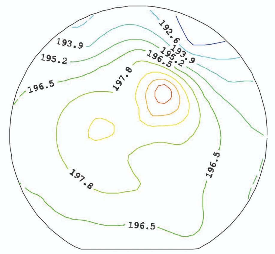
Sheet resistance map of an AlScN/GaN HEMT structure deposited on a 100 mm sapphire wafer. The average sheet resistance is 197 Ω/square, with a standard deviation below 1 percent.
We started our work on AlScN by discussing the potential precursors for scandium with our supplier of specialty chemicals. In addition – and what probably contributed to our success – we calculated the temperature that the precursor would need to be heated to for the growth of alloys of scandium nitride. This revealed a rather challenging result: the temperature of the gas mixing system has to be so high that it is beyond the reach of all the MOCVD reactors on the market. But this did not deter us. Some of those within our team have experience with MOCVD equipment, and we were also able to seek advice from several manufacturers of MOCVD components. Drawing on all of this, we designed our own gas mixing system, identifying the right components and settings.Since then, we have passed many milestones. Following several months of testing, we can now produce the alloys we intend to, which incorporate 20 percent to 30 percent of scandium. And thanks to the great experience of the structural characterisation team, we have uncovered the optimum growth conditions for forming the pure wurtzite phase of AlScN. Our focus is now on improving material quality and purity, as well as increasing the productivity of the epitaxial growth process.
The progress that we have made has led us to file a patent application for the growth of materials by MOCVD, using precursors with very low volatility. We hope that the design that we have developed will be very useful to the manufacturers of MOCVD equipment, and that some of them will soon adopt it in their tools. If they do, this could increase the number of researchers that work with AlScN in laboratories and industries.
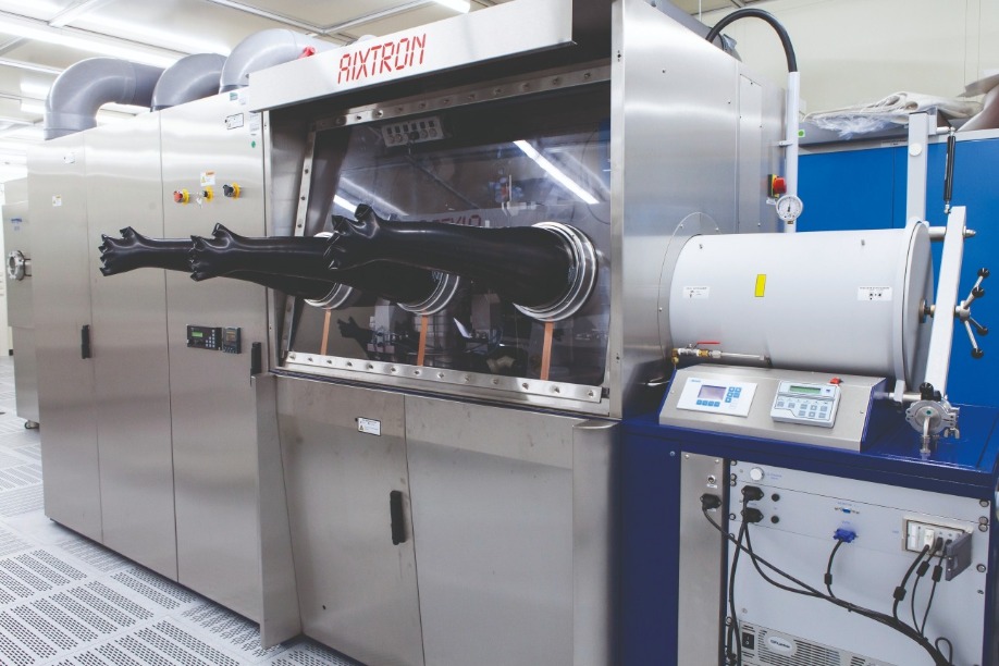
The MOCVD system at Fraunhofer IAF has been modified by the research group to enable the growth of AlScN with sufficient quality and productivity for industry.
Recently, we produced our first HEMT structures and started fabrication of devices. Our first GaN/AlScN heterostructures had a sheet resistance of 200-500 W/square, mobilities close to 900 cm2 V-1 s-1, and sheet carrier densities of 2-5 x 1013 cm-2.While these values are encouraging, far better results are possible by improving crystal quality. In particular, we want to reduce the roughness of our epitaxial heterostructures. The roughness is still higher than typical AlGaN/GaN structures. In addition, we will look to improve the purity of the AlScN layers, as they have high carbon and oxygen levels – these impurities may be detrimental to HEMT structures and other applications. One of today’s projects is to test various growth parameters and see if they can improve the quality of the AlScN epitaxial layers.
A goal for the future is to try and identify new precursors. We expect that by using different ligands in the scandium precursors we can enhance the volatility of this material, and ultimately increase the growth rate from its current value of only 0.1 µm/h. A hike in the growth rate is required before the process can be transferred to multi-wafer MOCVD reactors and used for high-volume production. Before that can take place, it is essential to investigate the impact of different precursors on the purity of the layers.
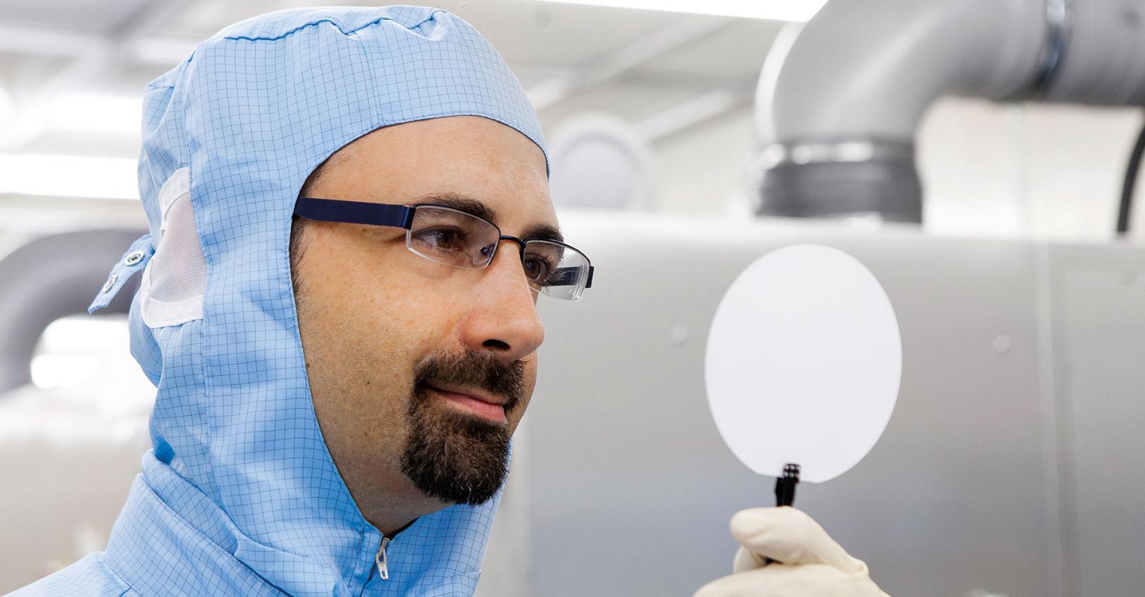
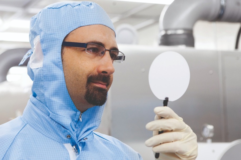
Scientists at Fraunhofer IAF are the world’s first to report the production of aluminium scandium nitride via MOCVD.
Opportunities for AlScNThere are many great opportunities for AlScN. It has the potential to be the leading material in power and high-frequency electronics, serving in radar, inverters for photovoltaics, and in inverters and converters in electrical vehicles.
But that’s by no means the limit for the use of AlScN. It can feature in filters for 5G, where it can deliver higher performance, thanks to high electromechanical coupling of AlScN. When this is used in electroacoustic components, such as surface acoustic wave, bulk acoustic wave and other types of resonators, magnetron sputtering can deposit films of sufficient quality. This technique, which we have even employed in our institute, has been used to make commercial RF front-end components that have alloys containing scandium. However, if MOCVD is used, the quality of the AlScN layers is better. What is not clear is how valuable this improvement is, and how a switch from sputtering to MOCVD will impact the cost of the filter, and its competitiveness in the market place.
Another amazing property of AlScN is its high degree of ferroelectricity. This attribute could see it adopted in mass storage devices, micro-mechanic actuators, and non-linear optical devices. HEMTs that are made with AlScN can be benefit from its ferroelectric characteristics, as this could allow the reduction in short-channel effects in ultra-scaled transistors, and even enable this device to switch, by using an electric field to invert the polarity of the AlScN barrier layer.
There are further opportunities for AlScN-based materials in optoelectronics. According to theoretical calculations, alloying GaN with ScN and YN can double the internal quantum efficiency of LEDs. If these alloys are used to make efficient multi-quantum wells emitting in the green, this could be a solution to the ‘green gap’, a spectral domain that is not well served by InGaN-based and AlGaInP-based LEDs.
Last but not least, the capability to grow AlScN by MOCVD could enable the growth of other ‘exotic’ materials that have, up until now, only been investigated in research laboratories. It is possible that nitride magnetic materials, such as the nitrides of gadolium and europium, could be manufactured with a similar setup to ours.
While we continue to explore the possibility and potential of AlScN, we are actively searching for research and industrial partners to increase the work undertaken on scandium-containing nitrides. This alloy has great potential, and there is still much to investigate and discover. The exciting journey has only just begun.
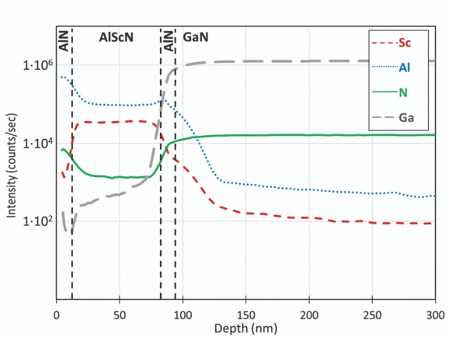
SIMS analysis of a 70 nm-thick Al0.7Sc0.3N layer deposited on a GaN/Al2O3 template with a 10 nm-thick AlN spacer and a 5 nm AlN cap.
T. E. Kazior et al. presented at IEEE/MTT-S International Microwave Symposium, Boston, USA, 2019.
A. J. Green et al. IEEE Electron Device Lett. 40 1056 (2019)
M. T. Hardy et al. Appl. Phys. Lett. 110 162104 (2017)
K. Frei et al. Jpn. J. Appl. Phys. 58 SC1045 (2019)
S. Leone et al. Metalorganic chemical vapor deposition of aluminium scandium nitride , DOI: 10.1002/pssr.201900535.


