
Crystal phase tuning creates new functionality
Lead Image : Photo by Simon Hönl
Metastable crystal phases exhibit highly desirable properties, with potential benefits including a solution to the ‘green gap’ and group IV materials with a direct band gap
BY PHILIPP STAUDINGER, KIRSTEN MOSELUND AND HEINZ SCHMID FROM IBM RESEARCH
When device performance is not good enough, researchers wrack their brains, trying to figure out a way to deliver a substantial improvement. Radical approaches often appeal, such as replacing the existing material system with another. This can pay dividends, as has been shown in the space solar cell market, where a switch from silicon cells to those made from multiple junctions, featuring germanium, InGaAs and InGaP, has delivered a boost in efficiency.
But there is another, more subtle approach, also with much promise. Rather than discarding the material system, it can be modified by transforming its crystalline phase. In this way the physical properties of an abundant, well-studied semiconductor can be fine-tuned, while making only minimal changes to its chemistry, which provides the advantage that established fabrication technology can still be used in existing fabs. This is the approach that we are pursuing at IBM, where we have broken new ground by developing novel processes to control the crystal phase in planar films.
In order to appreciate the advances that we have made, it is critical to grasp the basics of crystal structures in semiconductors. Fortunately, this is not too hard, as there are only two predominant crystal symmetries to consider. These are the cubic and hexagonal forms. Note that for elemental semiconductors they are referred to as diamond and lonsdaleite, while for compounds, zinc-blende and wurtzite are used, respectively (see Figure 1).
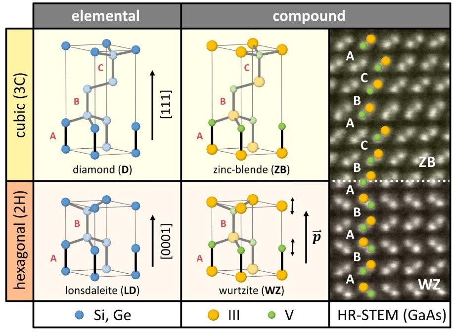
Figure 1. The difference between the cubic (3C) and the hexagonal (2H) crystal symmetries is defined by the atomic bilayer stacking along the [111] or [0001] direction. The corresponding phases are called diamond and lonsdaleite for elemental semiconductors, and zinc-blende and wurtzite for compound semiconductors. The loss of symmetry combined with the ionicity results in spontaneous polarization effects in wurtzite semiconductors, which are absent in other symmetries. A high-resolution scanning transmission electron microscopy image reveals the zinc-blende and wurtzite configurations of GaAs, and shows that a transition between these two phases is possible along the stacking axis.
One way to view the difference between the two symmetries is to consider the bilayer stacking order along a particular crystallographic direction. In diamond or zinc-blende phases, stacking is ABCABC… along the [111] direction, which is the space diagonal of its cubic unit cell. In the hexagonal form every third layer is absent, creating ABAB… periodicity along the newly defined [0001] direction.When nanostructures are grown along this direction, switching the stacking order introduces a different crystal phase – and ultimately creates a new type of metastable material. This principle is illustrated in a high-resolution scanning transmission electron microscopy image of polymorphic GaAs (see right hand side of Figure 1). Note that this type of phase transition, involving a metastable state, is often observed in nanowires. It stems from their low-dimensional character, and the strong role that surface energies exert during epitaxial growth.
Metastable merits
Until recently, metastable crystal phases have often been viewed as just a curiosity of nanowire growth. But now they might potentially provide solutions to some of the biggest problems associated with compound semiconductor devices. In conventional GaN LEDs, which have a wurtzite crystal structure, radiative recombination is impaired by strong internal fields that are responsible for the quantum confined Stark effect. Switch to the cubic phase, and these fields go away, helping to bridge the ‘green gap’ – a wavelength range in the centre of the visible spectrum that so far lacks efficient emitting materials.
Another promising solution to address the green gap is to use metastable wurtzite III-phosphides, as this class of III-Vs offers an extended tuneable direct bandgap throughout the visible spectrum in contrast to their stable counterparts (see Figure 2). Equally exciting is that germanium and germanium-rich SiGe compounds become direct bandgap semiconductors in their metastable lonsdaleite phase. This could open the door to CMOS-integrated light sources for on-chip optical communication.
These opportunities highlight the promise that crystal phase tuning has, to deliver a profound impact on many sectors within our industry, including electronics and solid-state lighting. Progress is not easy, however, as growth of metastable phases is extraordinarily challenging. For too long, success has been limited to thin nanowires, which are notoriously difficult to turn into devices, hampering scientific and commercial exploitation. What’s needed are technologies that will enable the synthesis of these materials in sizes and form factors that are compatible with conventional processing techniques.
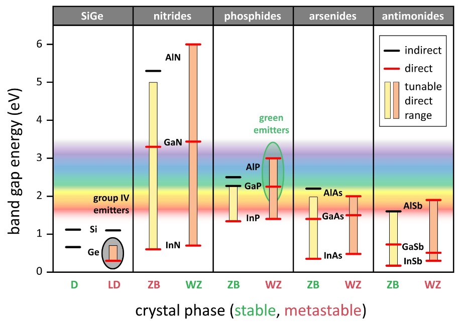
Figure 2. Bandgap energies of common semiconductors differ in their stable and metastable phase. For each semiconductor, the left side depicts the cubic phase, and the right side the hexagonal phase. Except for nitrides, the cubic phase is thermodynamically preferred. The hexagonal symmetry generally offers a wider range of direct bandgaps. Silicon is an exception, staying indirect even in the lonsdaleite phase. Crystal phase tuning offers an extended range for wurtzite III-phosphides throughout the visible spectrum and a direct group IV lonsdaleite SiGe compound for compositions of up to around Si0.35Ge0.65.
Unfortunately, due to thermodynamics, materials that are grown at typical temperatures for epitaxy tend to find their energetical minimum in their stable configuration. That’s particularly the case for the deposition of extended layers, as bulk properties dominate in this regime. So materials have to be tricked into crystallizing in a metastable phase. Fortunately, if this happens, they will then remain in that configuration, due to the large energy barrier that prevents atomic re-arrangement.Over the years, many groups have investigated different techniques for producing metastable material using either MBE or MOCVD. In general, these approaches are based on the transfer of the crystal phase from a substrate to an epilayer, which – under the right conditions – forces the layer to adopt its metastable form. The downside of this approach is that there are no appropriate substrates with lattice constants that are suitable for the materials of interest. Consequently, these films tend to be plagued by large defect densities, making them unsuitable for device applications.
 Photo by Elisabetta Corti
From nanowire to film growth
We are taking a different approach, based on novel epitaxial techniques that build on the knowledge of nanowire growth. Our aim is to produce high-quality metastable films, which provide a platform for robust material characterisation and device fabrication.
Our success comes from exploring a range of strategies. Initially, we studied selective-area epitaxy. Although this did not produce metastable layers, it did provide a foundation for more elaborate methods, making use of either a zipper-like growth mode or confinement under a top oxide (see Figure 3 for details).
Progress has come from the use of conformal epitaxy, which is described in more detail in Figure 4. Our starting point is a conventional zinc blende III-V substrate that is patterned in lines, using an oxide mask. Sacrificial etching defines hollow cavities, which have openings on their extremities to allow growth species to diffuse inside. MOCVD is employed for this, as it allows selective nucleation in the centre of the template. After this, the growth of the crystal is guided within the cavity.
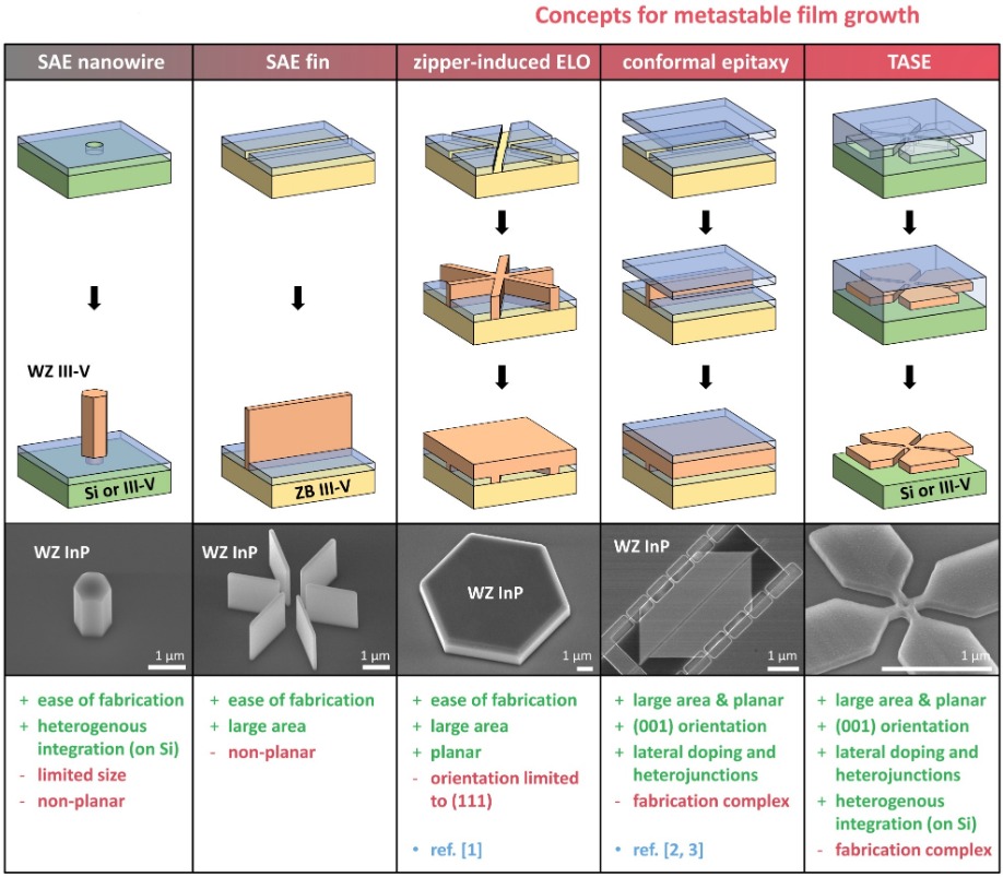
Figure 3. Several strategies can be used for wurtzite epitaxy, from nanowire to film growth. Selective-area epitaxy (SAE) of nanowires and fins allows for a phase change along the vertical stacking axis. The team at IBM have used this principle as a basis for other more elaborate techniques to obtain planar films. Connected fins can result in a zipper-induced epitaxial lateral overgrowth, as detailed in [1]. Conformal epitaxy makes use of a physical layer confinement, realized via an oxide layer on top of the seed line. This enables the use of standard (001) oriented substrates [2, 3]. Starting growth from a small seed additionally allows for direct growth on silicon wafers, accomplished by template-assisted selective epitaxy (TASE). Such an approach also allows for the growth of more advanced geometries, rather than just layers.
This approach has many advantages. Its greatest strength is that by selecting the substrate orientation and the orientation of the line openings, we exert full control over the growth direction of the crystal. This allows us to manipulate bilayer stacking, to ultimately engineer a phase transition. Another merit of our approach is that by forcing a non-vertical growth front, we can employ standard (001) substrates when growing along the [110] direction.Last but by no means least, our technology allows us to choose the geometry of the crystal through the design of the cavity. As well as being able to produce a flat top surface, which is compatible with standard film processing techniques, we can produce geometries beyond simple rectangles, such as those that form optical resonators. The lateral growth direction further opens up the opportunity for in-plane integration of heterostructures and offers great promise for device fabrication.
Going big
While there is much to admire about conformal epitaxy – it offers control over growth conditions and substrate orientation, and has additional advantages, such as lateral doping profiles and the co-integration of multiple materials – it does have its drawbacks. Its biggest weakness comes from its elaborateness.
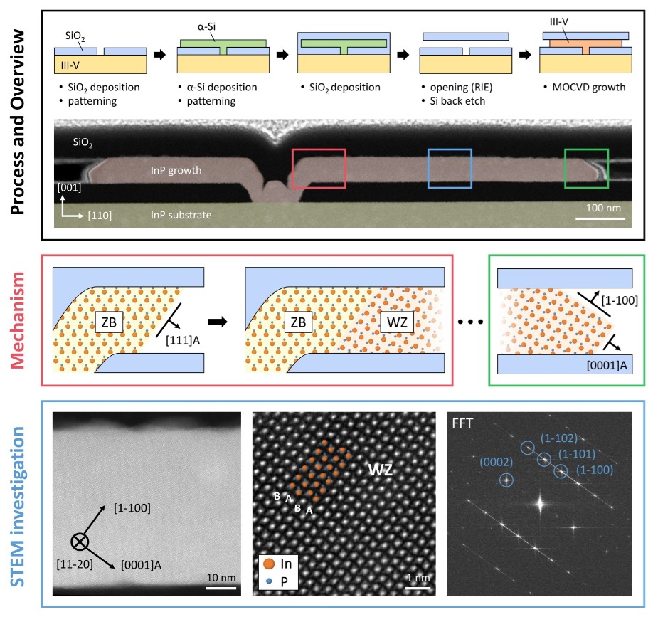
Figure 4. The team at IBM have used conformal epitaxy to produce metastable films. Processing steps involve a sacrificial material – typically amorphous silicon – to form an empty oxide cavity on top of a III-V wafer. Subsequent selective epitaxial growth in the cavity, using MOCVD, can then proceed, starting from a line opening in the oxide. A cross-sectional, false-coloured, scanning transmission electron microscopy image shows a typical InP structure with a dip on top of the line seed that results from processing. Coloured rectangles, showing areas of interest, are described in more detail. In the first section of the grown material, pure zinc-blende material is obtained, mirroring the crystal structure in the substrate, because epitaxy follows directions other than the stacking axis of the atomic bilayers. Once the [111] facet is formed, a phase transition can take place under the correct growth conditions. This enables a deposition that is similar to fin-growth with a [0001]A growth front and a [1-100] side facet. The bottom row depicts a detailed high-resolution, scanning transmission electron microscopy investigation of the central area. The wurtzite phase can be seen directly in the atomic stacking as well as in a fast Fourier transformation (FFT) image to the right.
There is the need for careful preparation of the substrate and multiple fabrication steps. However, despite these difficulties that impact cost and throughput, this type of approach can be compelling in advanced applications. In these situations, we recommend a variant known as TASE – short for template-assisted selective epitaxy (for details, see Figure 3). It also enables lattice-mismatched hetero-integration on standard silicon substrates.We have also pioneered a technique for producing layers in an economical way: zipper-induced epitaxial lateral overgrowth (this is illustrated in Figure 3). This involves selective-area epitaxy on (111)-oriented wafers and delivers a change in the atomic stacking of bilayers along the vertical direction through the use of nanowires and fins. This type of low dimensional nanostructure, illustrated in Figure 5, tends to grow vertically, so it doesn’t expand laterally to form a layer. However, with a small trick, we can create an unstable concave edge during growth. This edge triggers a zipper point, leading to controlled lateral expansion. To do this, we merge, in a central point, line openings with directions that are different but crystallographically equivalent. As the lateral growth direction is perpendicular to the stacking axis, this prevents any additional phase change, ensuring that the metastable material is transferred into a layer.
With this elegant technique we have realised exceptional material quality and phase purity. Photoluminescence measurements, presented in Figure 5, demonstrate that the hexagonally shaped films are optically active. Light is emitted in a spectral domain that has been predicted for the metastable wurtzite phase of InP. Thanks to the robustness of our technique, many individual hexagons can be tiled together to produce a virtually continuous film of metastable material. This highlights the potential of our technology for making large-area virtual substrates, and promises to speed its use in applications.
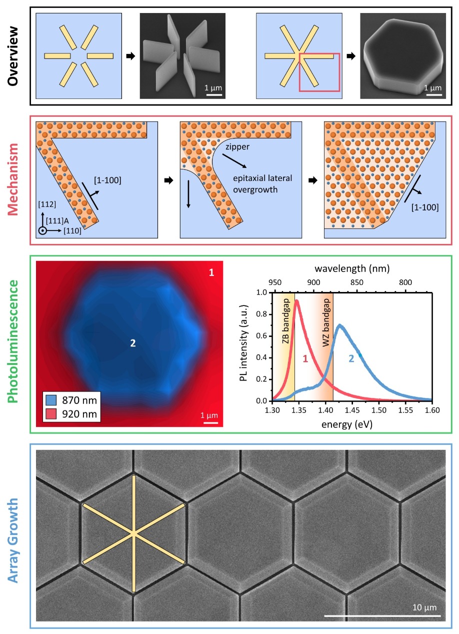
Figure 5. Zipper-induced epitaxial lateral overgrowth is a promising approach to scale the production of metastable films. Connecting the central point of circularly arranged metastable fins induces zipper points at the concave edges. In turn, this triggers epitaxial lateral overgrowth. In this unique epitaxy technique lateral growth continues until stable [1-100] edges are formed, resulting in the formation of hexagonal layers. Scanning micro-photoluminescence measurements reveal the emission difference between the substrate (zinc-blende) and the grown structures (wurtzite), formed in InP. Tiling individual hexagons closely together in an array results in a virtual wurtzite substrate. This can provide a platform for device applications.
Our research, along with that of some of our peers, is laying the groundwork for further development of substrates made from metastable phases of well-established semiconductors. While many challenges still need to be addressed, including the growth of ternaries and quantum wells and the formation of electrically driven devices, much progress has been made in the last few years. Due to these successes, we are optimistic that some of these conventional materials, given a new twist, will soon find their way into fabs.The work presented here received financial support from the European Union H2020 program SiLAS (Grant Agreement No. 735008)
Photo by Markus Ritter
Further reading
[1] P. Staudinger et al. Nano Lett. 20 686 (2020)
[2] P. Staudinger et al. Nano Lett. 18 7856 (2018)
[3] P. Staudinger et al. in 2019 Compound Semiconductor Week (CSW) 18, 1–2 (IEEE, 2019)


