
Plessey partners with Axus to deliver microLED displays
Companies develop CMP processes to enable Plessey’s monolithic GaN-on-Si technology
Plessey has announced a partnership with Axus Technology, a provider of CMP, wafer thinning and wafer polishing surface-processing solutions for semiconductor applications, to bring high-performance GaN-on-Silicon monolithic microLED technology to the mass market.
Plessey continues to invest heavily in its manufacturing facility to boost their proprietary microLED display capabilities with the purchase of metal and oxide chemical mechanical polishing (CMP) and associated tools from Axus to enable the wafer-scale bonding of microLED wafers to high-performance CMOS backplanes.
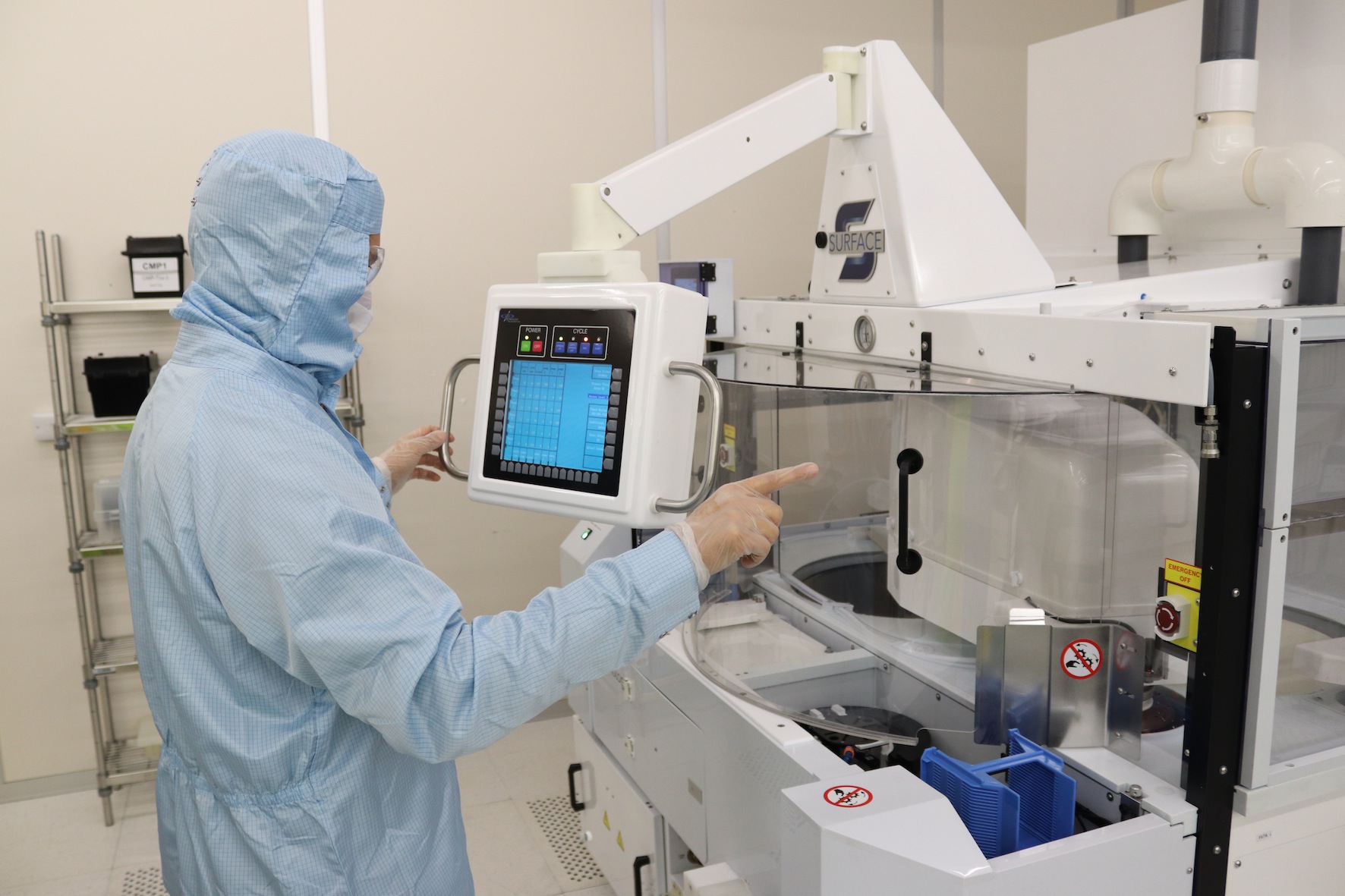
A number of Axus CMP and Scrubber systems have been deployed to enable critical wafer planarisation and preparation for wafer-scale bonding. Wafer-level bonding poses significant technical challenges and even with the right equipment requires extensive know-how and refined processes. Shortly after installation of the systems in 2019, Plessey achieved the world’s first functional wafer-level bonded GaN-on-Si monolithic 1080p 0.7 inch diagonal 8-micron pixel-pitch microLED active-matrix display.
Plessey has further optimised these systems and processes to achieve a successful wafer to wafer bond of a much smaller monochrome native Green 1080p microLED display 0.26 inch diagonal to a 3-micron pixel-pitch backplane display system engineered by Compound Photonics, creating over two million individual electrical bonds.
The formation of the Plessey/Axus partnership has led to the development of critical CMP processes for various materials key to enabling Plessey’s proprietary monolithic GaN-on-Si technology.
Engineers from both companies have collaborated to successfully accomplish these objectives at both Axus’ CMP foundry located in Chandler, Arizona and Plessey’s semiconductor fabrication facility in the United Kingdom.
In the future, the partnership will support scaling the technology for high-volume manufacture on the existing Axus equipment set and in the near future Axus’ new state-of-the-art, high flexibility/throughput Capstone CMP System, released to the market in late 2019.
Dan Trojan, president of Axus Technology, said: “We are honoured that Plessey has been able to achieve these key microLED technology advancements with the help of our tool platforms and process engineering capabilities and resources. We’ll be working closely with Plessey’s engineers for upgrades to their current tooling and subsequently scaling the technology on Capstone.”
Mike Snaith, CEO at Plessey, explained: “With our innovative approach and determination these tool platforms are enabling Plessey to advance its proprietary GaN on Silicon monolithic microLED technology. Our ever-expanding investment in our manufacturing facility in the UK is allowing Plessey to innovate rapidly and deliver leading-edge technology for AR and other display applications.”
MicroLED technology is continuing to emerge as the most likely successor to today's smart high-performance display applications, making displays with smaller form factor, even brighter and more power-efficient than current display technologies available.


