
Qromis: ready for business
As the GaN market gathers momentum, Qromis is serving up fab-friendly substrates and epi-wafers to ease device manufacture.
In January this year, Silicon Valley based Qromis, revealed two developments that signal the company is on the cusp of rapid expansion.
For starters, the fabless, wide bandgap materials business has just received an undisclosed investment from The Mirai Creation Fund, led by Japan-based investors SPARX.
At the same time, it has also signed a licensing agreement with Shin-Etsu Chemical, a Japan-based Silicon wafer and materials manufacturer, to manufacture substrates and epi wafers for GaN power/RF electronics, LED devices and more.
Qromis' latest developments follow five years of development of its novel materials technology for substrates,. And right now, chief executive, Cem Basceri, is excited.
“We've developed this unique CMOS fab-friendly substrate technology that is scalable and stress-matched to GaN,” he says. “It sounds simple but it's taken years of development and investment.”
“Now, a device manufacturer can take our substrate, and without any challenges, make many different device features,” he adds. “This is extremely valuable.”
Rapid progress
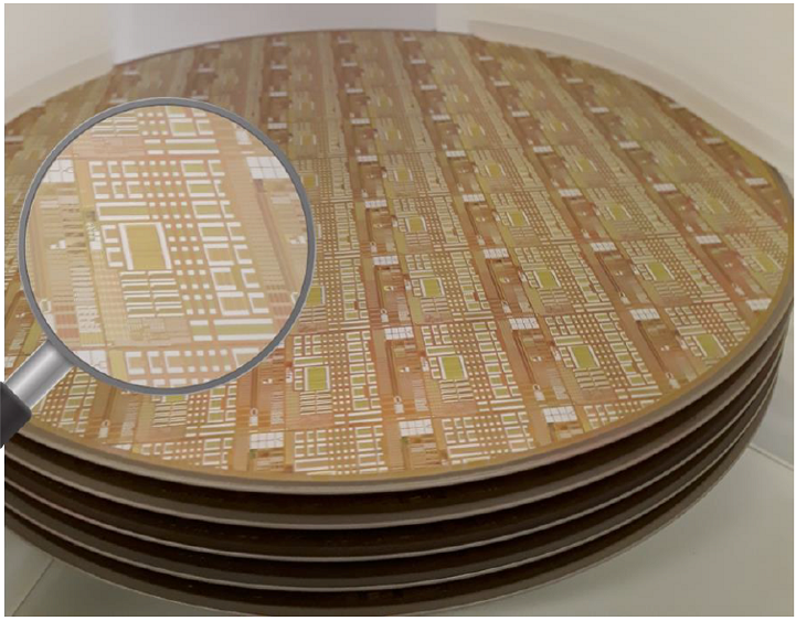
Qromis launched back in 2015 to commercialise its Qromis Substrate Technology, QST. Ready for GaN epi-growth, these substrates comprise an engineered Coefficient of Thermal Expansion (CTE)-matched core onto which several engineered layers are deposited. A top thin silicon interface is also deposited onto the engineered layers.
Crucially, the CTE-matched core has a thermal expansion that closely matches the thermal expansion of the GaN-AlGaN epitaxial layers, enabling the deposition of low dislocation density, crack-free GaN epitaxy from a few microns to bulk-like thickness.
As Basceri highlights: “We did this so that the substrate would be stress-matched with GaN without any cracking or wafer breakage issue and also to prevent substrate cross-talk in integrated circuits, which is a big issue on silicon.”
Qromis has already released six- and eight-inch GaN-ready QST substrates as well as six- and eight-inch 'templates' with 5 µm and 10 µm GaN layers. What's more, 200V and 650V GaN HEMT epi-wafers, based on six- and eight-inch QST substrates, are being fine-tuned for commercial devices while 900V and 1200V GaN HEMT epi-wafers are also being developed and sampled.
The company's rapid technology development follows partnerships and collaborations with a host of industry players, up and down the supply chain. Within a year of launching, the company had partnered with Vanguard International Semiconductor, licensing its key technologies to the Taiwan-based silicon foundry for manufacturing.
Since 2016, the company has also worked closely with microelectronics innovation hub, imec, Belgian, on device fabrication, developing GaN power devices, in discreet and monolithically-integrated ICs forms, on 200 mm QST substrates in an advanced CMOS silicon pilot line.
Imec and Qromis have also been collaborating with GaN MOCVD equipment manufacturer, Aixtron, Germany, on GaN-on-QST epitaxy development. The results have been quite remarkable.

Cem Basceri, Founder, President and CEO of Qromis
As Basceri points out, the industry standard platform for GaN-on-silicon has been 150 mm wafers. And while imec has pioneered the development of 200 mm GaN-on-silicon wafers for HEMTs to 650 V operating voltages, thermal mismatches between the GaN/AlGaN layers and silicon has stymied device fabrication at higher voltages.
Imec and Qromis have since developed enhancement mode p-GaN discrete and IC power devices on 200 mm QST substrates with epitaxy layers grown in Aixtron's G5+ C 200 mm MOVCD platform. Crucially, imec was able to port its p-GaN e-mode power device technology to Qromis' 200 mm GaN-on-QST wafers in its silicon pilot line, and also demonstrate high performance power devices.
“Vanguard then decided to licence imec's device technology, GaN power epitaxy and processes and the company is currently manufacturing and tuning devices to [partner's] specifications,” says Basceri. “This has been a big turning point.”
Ramping manufacture
In line with healthy GaN growth forecasts, Basceri says Vanguard will 'open its doors to everybody' later this year, offering GaN power, and later RF, device manufacturing services on the 200 mm diameter QST platform. This has also prompted the Qromis chief executive to establish a second manufacturing source for QST substrates and GaN-on-QST epitaxy wafers, in the form of Shin-Etsu Chemical. Importantly, with this partnership, QST-based materials products will be commercially available from both Shin-Etsu and Qromis for industry players
According to Basceri, Shin-Etsu is going to aggressively move ahead with the development of GaN-related products, supplementing its existing line-up of GaN-on-silicon, SOI and silicon wafers. As he says: “From what we hear from our partners and customers that use Vanguard, we are expecting wafer demand to reach tens of thousands of wafers in the next three to four years.”
With its substrates, Qromis will address a range of applications starting with GaN power and RF devices and later LED devices, such as microLEDs, and sensors. One of the key markets will be electric vehicles - as Basceri points out, a significant portion of SPARX's Mirai Creation Fund comes from Toyota Motor Corporation, which is heavily entrenched in this market.
“We expect to start ramping up 200 mm manufacturing between 2021 and 2022, and I would also expect to see an overall demand for 300 mm wafers starting by 2025 for which we have already started to receive some initial inquiries,” says Basceri. “Several years ago, there were missing links in the GaN business, but the tipping point is now here.”


