
EVG opens Heterogeneous Integration Centre
Combines wafer bonding, thin-wafer handling, lithography expertise, and pilot-line production facilities at HQ in Austria
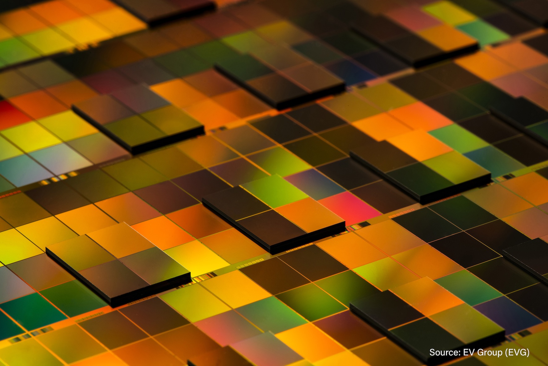
EV Group (EVG), a supplier of wafer bonding and lithography equipment for the MEMS, nanotechnology and semiconductor markets, has established the Heterogeneous Integration Competence Centre, which is designed to assist customers in using EVG's process solutions and expertise to enable new and enhanced products and applications driven by advances in system integration and packaging.
The Heterogeneous Integration (HI) Competence Centre combines EVG's wafer bonding, thin-wafer handling, and lithography products and expertise, as well as pilot-line production facilities and services at its state-of-the-art cleanroom facilities at EVG's headquarters in Austria, supported by EVG's worldwide network of process technology teams.
"Heterogeneous integration fuels new packaging architectures and demands new manufacturing technologies to support greater system and design flexibility, as well as increased performance and lower system design costs," stated Markus Wimplinger, corporate technology development & IP director of EV Group. "EVG's new HI Competence Centre provides an open access innovation incubator for our customers and partners across the microelectronics supply chain to collaborate while pooling our solutions and process technology resources to shorten development cycles and time to market for innovative devices and applications enabled by heterogeneous integration."
EVG has an extensive background in heterogeneous integration, providing solutions for this technology trend for more than 20 years. Among these are: permanent wafer bonding -including direct fusion and hybrid bonding for 3D packaging and metal bonding - and die-to-wafer bonding with and without collective carriers for integration of III-V compound semiconductors and silicon as well as high-density 3D packaging; temporary bonding and debonding, including mechanical, slide-off/lift-off, and UV laser assisted; thin-wafer handling; and innovative lithography technologies, including mask aligners, coaters and developers, and maskless exposure/digital lithography.
Advanced Packaging Milestones
In the field of permanent bonding, EVG pioneered the patented SmartView® wafer-to-wafer alignment system more than 20 years ago, and has refined this technology over the years to support breakthrough technology advances such as backside-illuminated CMOS image sensors (BSI-CIS) and more recently the first demonstration of sub-100-nm wafer-to-wafer alignment overlay for hybrid bonding - enabling devices such as 3D BSI-CIS and memory-on-logic stacking. EVG developed the first temporary bonding systems for ultra-thin wafers as early as 2001, which are essential for 3D/stacked die packaging, as well as revolutionised low-temperature laser de-bonding for ultra-thin and stacked fan-out packages.
In lithography, EVG cemented its position as a recognised technology leader with the delivery of the first UV muolding solutions for high-volume production of wafer-level optics more than a decade ago, and has since led the proliferation of nanoimprint lithography (NIL) to high-volume manufacturing (HVM). EVG continues to break speed and accuracy barriers in mask alignment lithography for advanced packaging and, more recently, unveiled the world's first highly scalable maskless exposure technology, which addresses emerging requirements in HVM back-end lithography.


