
On-chip nanowire laser shows high coupling efficiency
Chinese team shows 58 percent fractional power from CdS laser channelled into SiN waveguide
In the past decade, on-chip nanophotonics has attracted increasing attention for the realisation of integrated photonic circuits with faster operation, broader bandwidth, lower power consumption and higher compactness. While on-chip nanophotonic devices and circuits have been successfully fabricated CMOS -compatible technique, on-chip light sources remain challenging.
On the other hand, bottom-up grown semiconductor nanowires have long been used for nanoscale waveguide lasers. In recent years, increasing attention has been paid to the integration of active nanowires with on-chip planar waveguides for on-chip light sources. However, due to the large discrepancy in fabrication techniques, refractive index and geometric compatibility between a freestanding nanowire and an on-chip planar waveguide, a variety of issues, including a relatively low coupling efficiency, ineffective mode selection and low reproductivity, have yet to be addressed.
In a new paper published in Light Science & Application, scientists from the State Key Laboratory of Modern Optical Instrumentation, College of Optical Science and Engineering, Zhejiang University, China demonstrated an on-chip single-mode CdS nanowire laser with high coupling efficiency. The mode selection is realised using a Mach-Zehnder interferometer (MZI) structure.
Benefitting from the diversity of the available nanowire materials and high flexibility for bandgap engineering, the on-chip integration scheme demonstrated here can be readily extended to realise on-chip nanolasers from the ultraviolet to near-infrared ranges, which may offer new opportunities for both semiconductor nanowires and on-chip photonic devices.
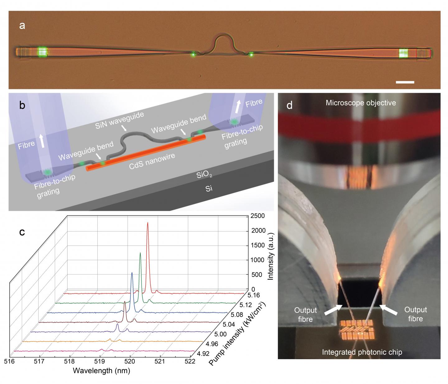
The image above shows: a, optical image of a hybrid MZI structure under excitation. b, the schematic configuration of the on-chip nanowire laser. A CdS nanowire is used as the gain material and is evanescently coupled to an ?-shaped SiN waveguide at both sides to form a hybrid MZI structure. In the coupling area, SiN waveguide bends are predesigned to ensure a high coupling efficiency with excellent reproducibility. Fibre-to-chip grating couplers are designed at both ends of the SiN waveguide, which couple the laser signal from the on-chip SiN waveguide into standard optical fibres for optical characterisation. c, Lasing spectra obtained at different pumping intensities above the threshold. The dominant lasing peak is centred at a wavelength of approximately 518.9 nm with a linewidth of approximately 0.1 nm. The side-mode suppression ratio increases with increasing pumping intensity and realises a maximum value of approximately a factor of 20 (13 dB). d, optical image of the measurement setup under an optical microscope. The measurement setup uses output fibres to collect signals out of the chip via fibre-to-chip grating couplers.
These scientists summarise the fabrication and operational principle of the laser:
"We use micromanipulation under an optical microscope to integrate a CdS nanowire onto a SiN chip and form a hybrid MZI structure with excellent reproducibility. By using the MZI for mode selection, we operate the laser in single mode. We can also change the output ratios between the two ports of the lasing MZI by using different coupling lengths of the waveguide bends."
"The overall size of the hybrid MZI structure is kept below 100 μm. Fibre-to-chip grating couplers are designed at both ends of the SiN waveguide, which couple the laser signal from the on-chip SiN waveguide into standard optical fibres for optical characterisation." "By comparing the lasing output intensities from the nanowire end and the grating area, we estimate the fractional power channelled into the SiN waveguide to be approximately 58 percent, much higher than previous results obtained in chip integrated nanowire lasers, and can be further improved by optimising the coupling efficiency between the nanowire and the SiN waveguide." they added.
"Benefitting from the great diversity of the available nanowire materials and high flexibility for bandgap engineering, the on-chip integration scheme demonstrated here can be readily extended to realise on-chip nanolasers from the ultraviolet to near-infrared ranges, and the on-chip single-mode nanowire laser may thus offer an opportunity to develop on-chip physical and biochemical optical sensors with higher stability and compactness. " the scientists forecast.
'On-chip single-mode CdS nanowire laser' by Qingyang Bao et al; Light: Science & Applications volume 9, Article number: 42 (2020)


