
European team makes high-efficiency laser for silicon chips
Laser made of germanium and tin has efficiency comparable with conventional GaAs lasers
Scientists from Forschungszentrum Jülich say they have come a step closer to integrating lasers directly in silicon Together with researchers from Centre de Nanosciences et de Nanotechnologies (C2N) in Paris and the French company STMicroelectronics as well as CEA-LETI Grenoble, they have developed a compatible semiconductor laser made of germanium and tin, whose efficiency is comparable with conventional GaAs semiconductor lasers on Si. (Nature Photonics, DOI: 10.1038/s41566-020-0601-5)
Optical data transfer permits much higher data rates and ranges than current electronic processes while also using less energy. Computation and data centres, therefore, already default to optical fibre whenever cables exceed a length of about one metre. In future, optic solutions will be in demand for shorter and shorter distances due to increasing requirements, for example board to board or chip to chip data transfer. This applies particularly to artificial intelligence (AI) systems where large data volumes must be transferred within a large network in order to train the chip and the algorithms.
"The most crucial missing component is a cheap laser, which is necessary to achieve high data rates. An electrically pumped laser compatible with the silicon-based CMOS technology would be ideal," explains Detlev Grützmacher, director at Forschungszentrum Jülich's Peter Grünberg Institute (PGI-9). "Such a laser could then simply be shaped during the chip manufacturing process since the entire chip production is ultimately based on this technology".
"Laser components are currently manufactured externally and must be integrated subsequently, which makes the technology expensive," explains Grützmacher.
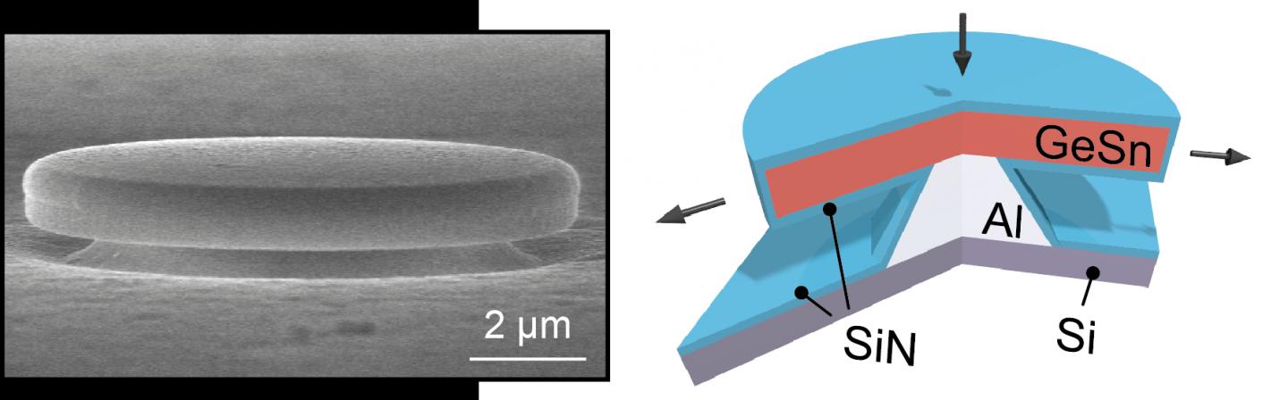
In contrast, the new laser can be manufactured during the CMOS production process. Back in 2015, Jülich researchers showed that laser emission can be obtained in GeSn system. The decisive factor in this is the high tin content: back then, it amounted to 12 percent, which is far above the solubility limit of 1 percent .
"Pure germanium is, by its nature, an indirect semiconductor like silicon. The high concentration of tin is what turns it into a direct semiconductor for a laser source," explains Dan Buca, working group leader at Jülich's Peter Grünberg Institute (PGI-9).
The patented epitaxial growth process developed by Jülich is used by several research groups all over the world. By further increasing the tin concentration, lasers have already been made that work not only at low temperatures but also at 0degC.
"A high tin content, however, decreases the laser efficiency. The laser then requires a relatively high pumping power. At 12-14 percent tin, we already need 100-300 kW/cm2," explains Nils von den Driesch. "We thus tried to reduce the concentration of tin and compensate this by additionally stressing the material, which considerably improves the optical properties."
For the new laser, the researchers reduced the tin content to approximately 5 percent - and simultaneously decreased the necessary pumping power to 0.8 kW/cm2. This produces so little waste heat that this laser is the first group IV semiconductor laser that can be operated not only in a pulsed regime but also in a continuous working regime, i.e. as a "continuous-wave laser".
"These values demonstrate that a germanium-tin laser is technologically feasible and that its efficiency matches that of conventional III-V semiconductor lasers grown on Si. This also brings much closer to an electrical pumped laser for industrial-application that works at room temperature," explains institute head Grützmacher. The new laser is currently limited to optical excitation and low temperatures of about -140degC.
Such a laser would be interesting not only for optical data transfer but also for a variety of other applications since there are hardly any cheap alternatives for the corresponding wavelengths in the infrared range of 2-4 μm. Potential applications range from infrared and night-vision systems all the way to gas sensors for monitoring the environment in climate research or even breath gases analyses for medical diagnosis.
'Ultra-low-threshold continuous-wave and pulsed lasing in tensile-strained GeSn alloys' by Anas Elbaz et al; Nature Photonics (2020)


