

Uniting III-Vs with silicon for beyond-5G front-end modules

Combining aspect ratio trapping with nano-ridge engineering enables 300 mm substrates to provide a platform for the fabrication of GaAs/InGaP HBTs that deliver amplification in the millimetre-wave
BY ABHITOSH VAIS FROM IMEC
FOR THE FIRST FOUR GENERATIONS of mobile communication technology, changes to the transmission frequencies have been evolutionary, rather than revolutionary. The operating frequency has moved up from just below a gigahertz to several gigahertz and the bandwidth has widened from tens of kilohertz to tens of megahertz.
Viewed in these terms, 5G is a radical departure from what has come before (see Figure 1). It will still involve some transmission at a few gigahertz – known as the sub-6 GHz bands – but in addition, it will use millimetre-wave frequencies, which are needed to address the bandwidth limitations at current frequency bands.
One of the downsides of using bands in the millimetre wave, such as those centred around 28 GHz and 39 GHz, is that they suffer from far greater attenuation. To address this, there needs to be an introduction of a network of small cells, as well as new designs for the handset, leading to an increased complexity in the front-end design.
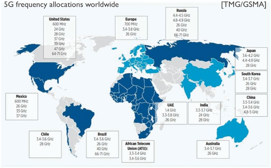
Figure 1. Frequency band allocations for 5G deployments across the world. [TMG/GSMA], https://www.gsma.com/spectrum/wp-content/uploads/2019/10/mmWave-5G-benefits.pdf
A key ingredient in today’s handsets is the GaAs/InGaP HBT, fabricated on expensive GaAs substrates. This class of transistor is used to make power amplifiers, which feature in separate modules, each covering a different frequency band.As 5G operating in the millimetre-wave domain is rolled out, the RF performance from these transistors must be maintained or even improved while lowering cost, increasing the flexibility in circuit design, and trimming power losses and the chip footprint. Unfortunately, existing commercial technologies are struggling to satisfy all these requirements for enabling a good RF front-end module, so there is a need to turn to innovative materials and device architectures.
At imec, we have developed a hybrid III-V/CMOS technology that promises to deliver the low form factor and low costs required for millimetre-wave RF applications. It harnesses the power handling (see Figure 2) and the linearity at high frequencies associated with III-V systems, while drawing on advanced CMOS back-end-of-line processes for the creation of complex control circuitry. What’s more, thanks to co-integration, there is the potential for improved energy efficiency for the overall circuit, leading to a power-efficient, low-cost millimetre-wave technology that could be produced in high volume.
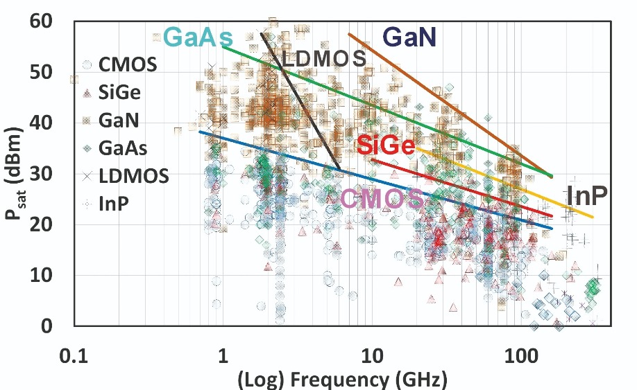
Figure 2. Technological trends in output power, Psat, for different technologies with respect to operating frequencies. Solid lines are only to guide the eyes. [H. Wang, et al., “Power Amplifiers Performance Survey 2000-Present,” [Online]. Available: https://gems.ece.gatech.edu/PA_survey.html]
One of the biggest challenges in uniting III-V materials, such as GaAs, with silicon is the large lattice mismatch. Epitaxial growth on a lattice-mismatched substrate leads to generation of defects – mainly threading dislocations. These imperfections induce an unwanted leakage current, degrading device performance.Some research teams have tried to lower the density of these defects by inserting a strain-relaxed buffer layer between the substrate and the device. However, there is a significant additional cost associated with adding layers of either SiGe, germanium or a III-V metamorphic stack that needs to be more than 10 µm-thick to reduce defect density to an acceptable value.
Whatever approach is used to create a CMOS/III-V technology, it must include standard silicon substrates to keep complexity and cost in check.
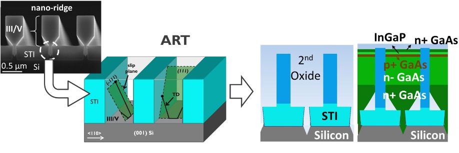
Figure 3. An illustration of the features of aspect ratio trapping (ART) and nano-ridge engineering to grow nano-ridges. Note that due to ART, the threading dislocations are trapped inside the narrow trench while a relatively defect-free nano-ridge is grown inside the second oxide.
Aspect ratio trappingOur approach combines aspect ratio trapping, where defects are confined to the bottom of narrow trenches, with nano-ridge engineering, which leads to an increased, defect-free III-V volume that can be used to fabricate devices (see Figure 3). Further processing of the nano-ridges, using a fully CMOS compatible flow, creates the final device (see Figure 4), and ultimately enables co-integration with silicon CMOS devices.
One of the strengths of this approach is that it enables the integration of silicon substrates and III-V materials without having to grow thick buffer layers or to turn to expensive substrates. In addition, we can draw on our expertise on III-V-on-300 mm silicon – developed in the context of CMOS scaling and silicon CMOS.
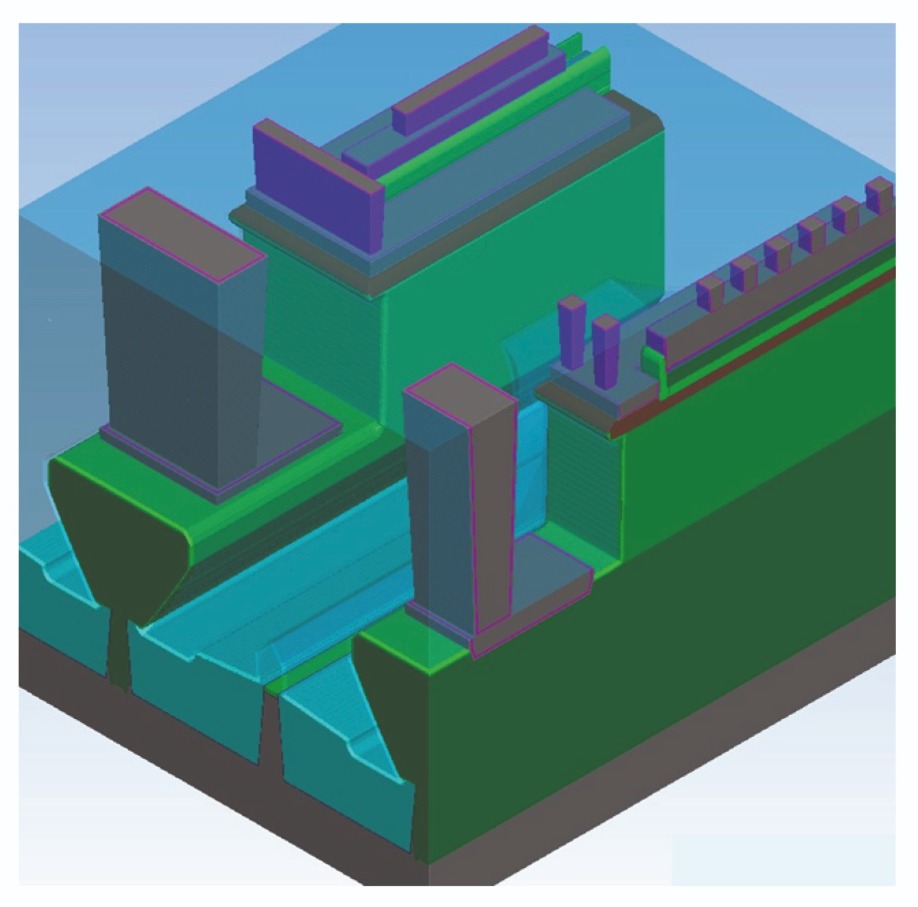
Figure 4. III-V HBTs can be integrated on a 300 mm silicon wafer using a CMOS-compatible process flow developed at imec.
We produce our nano-ridges by growing III-Vs on 300 mm silicon (001) wafers with a double-oxide structure (see Figure 4). The first SiO2 layer is a 400 nm-thick shallow trench isolation (STI) template. This features a pattern of narrow trenches that are 80 nm wide, and have a silicon {111}-faceted V-groove at the bottom. The pitch is 800 nm. On this we add a second oxide layer, which is 1000 nm-thick. Processing this creates 600 nm-wide trenches, centred on the narrow trenches below.
Using selective-area growth, we deposit III-V material in the narrow trenches. The large lattice mismatch between silicon and the III-Vs leads to the generation of defects, but they are confined to the bottom of this trench, thanks to its high aspect ratio. This ensures that the material growing out from the narrow trench is free from threading dislocations.
Our next step is to turn to nano-ridge engineering to widen the nano-ridge, so that a (001) growth facet can be maintained, enabling a flat interface. If nano-ridge engineering is allowed to grow a free-standing structure, a large box-like shape results. We avoid this by adding a second oxide template. Once the nano-ridge reaches the second oxide, sidewall deposition is reduced in the device’s active region.
Growth of the III-Vs on the processed 300 mm silicon wafers takes place in a low-pressure MOCVD chamber using standard liquid precursors for the group III and group V sources. Doping is realised with the addition of carbon tetrabromide and silane.
Note that as well as being able to produce traditional box-like growth of III-Vs on silicon, nano-ridge engineering can yield different shapes by carefully adjusting the growth conditions. This allows good control of the nano-ridge profile at the nanometre scale.
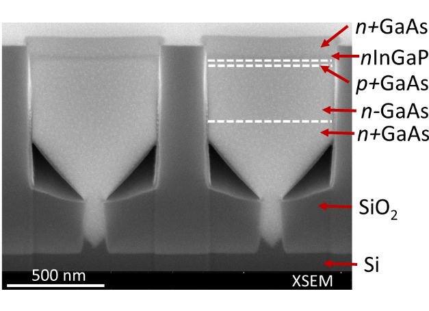
Figure 5. Cross-section scanning electron micrograph (XSEM) of the GaAs/InGaP nano-ridges grown on a 300 mm silicon substrate using nano-ridge engineering. Notice the absence of defects inside the active device stack.
Defect characterisationWe evaluate the effectiveness of our approach by analysing the defect density in the nano-ridge. One of the most common techniques for scrutinising material is transmission electron microscopy. We have used a form of this known as high-angle annular dark-field scanning. This technique, which can expose defects in the trench, reveals that the III-V device stack is free of misfit dislocations (see Figure 5 and 6). Although the standard form of transmission electron microscopy provides better accuracy in uncovering defects, it has a very small scanning area, making it rather cumbersome for a reliable determination of the defect density.
Another common technique for scrutinising material is electron channeling contrast imaging. It is a relatively fast option for generating a statistically relevant dataset. Using this technique, we have found that the threading dislocation density at the surface of the GaAs nano-ridges is below 3 x 106 cm-2. As the value of the defect density is limited by the inspection area, we envisage that the actual threading dislocation density in the GaAs nano-ridges could be even lower than this.
Based on this finding, we know that the threading dislocation density in our ridges is low enough to prevent it from having a significant impact on our devices.
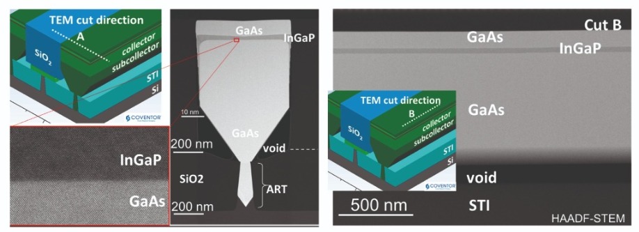
Figure 6. High-angle annular dark-field scanning transmission electron microscopy of the nano-ridge across the width (left) and along the length of the nano-ridge (right).
Epitaxial systems with mismatched lattice constants can also be riddled with planar defects. Our approach traps this form of defect in {111} planes parallel to the sidewalls, but when planar defects run perpendicular to the sidewall there is the possibility of them ending up in the device stack. Here, this density could be between 0.14 µm-1 and 0.45 µm-1. The good news, however, is that as planar defects do not involve open crystal bonds or a pronounced strain field, they will have less impact on device performance than dislocation defects.HBTs on 300 mm silicon
Drawing on our capability to grow defect-free III-V layers on silicon, we have recently demonstrated GaAs/InGaP HBTs that are monolithically integrated on a standard 300 mm silicon substrate. This success provides a stepping-stone towards the fabrication of InGaAs-based devices for beyond-5G applications.
Our breakthrough is based on a stack of n-InGaP/p-GaAs/n-GaAs layers that exhibit HBT characteristics. The emitter-base and base-collector diodes show ideality factors of around 1.2 and 1.4, respectively, highlighting the good quality of these junctions and the materials that form them. Additional evidence of the high material quality of this structure is a DC current gain of more than 110 and a breakdown voltage between the collector and base of 10 V.
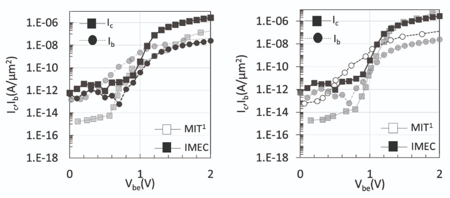
Figure 7. Comparison of electrical characterization (Gummel plots) of the devices fabricated in this work with that of reference devices [1] with strain-relaxed buffer layers (presented at IEDM 2019). [1] C. Heidelberger et al. Journal of Applied Physics 123 161532 (2018).
To benchmark our device, we compared its transfer characteristics with HBTs with a similar design that were formed on a 2-inch GaAs substrate and a thick strain-relaxed buffer layer with similar defect density (see Figure 7). Encouragingly, our device outperforms that made on the thick buffer, and its key traits are very similar to a device made on a high-quality 2-inch GaAs substrate (see Figure 8). This finding supports our claim that the quality of our material produced by nano-ridge engineering on 300 mm silicon is sufficient enough – we don’t need thick strain-relaxed buffer layers or expensive substrates.Thanks to our successes, we have high hopes for our technology. One of its strengths is that it shows how III-Vs and silicon CMOS can combine to serve 5G and millimetre-wave applications. This can be accomplished with InGaAs HBTs on a 300 mm silicon substrate, a combination that could find deployment in RF applications beyond 5G.
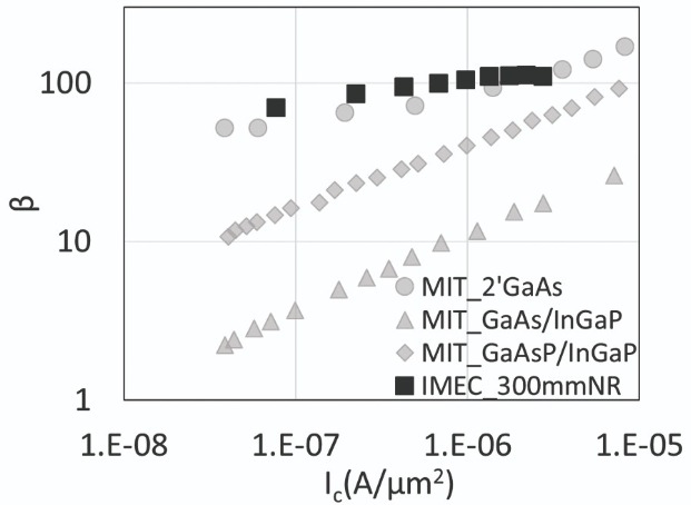
Figure 8. Comparison of DC current gain of the HBT devices fabricated on nano-ridge engineering based GaAs/InGaP stack with that of reference devices [1] with strain relaxed buffer layers (presented at IEDM 2019). [1] C. Heidelberger x. Journal of Applied Physics 123 161532 (2018)
We take great heart from the initial performance of our hybrid III-V/CMOS technology, which leads to devices with a comparable performance to those made on high-quality GaAs substrates, and we look forward to further explorations in nano-ridge engineering, to uncover its full potential.


