A better face for the SiC MOSFET

SiC MOSFETs with a V-grooved trench reduce on-resistance and trim switching losses.
BY Kosuke Uchida AND TAKASHI TSUNO FROM Sumitomo Electric Industries
When the leaders of the most powerful countries met at the World Economic Forum in January, one topic dominated the agenda – climate change. For many of them, this is by far the biggest issue of our age, with action needed right now to cut carbon footprints.
There are so many opportunities to do this. Some are at the national level, such increasing the number of nuclear power plants and solar farms. There are also changes that companies can make, such as investing is more efficient machinery, and there are personal decisions, such as moving to a more plant-based diet and taking fewer flights.
Within this mix, one of the options for saving energy and curbing carbon dioxide emissions is the introduction of more efficient power control technologies. They are widely deployed, playing an essential role in electric vehicles, in renewable energy systems, and in industrial motor drives.
Most of today’s power devices are made from silicon. Their performance has improved over many decades, but they are now encroaching theoretical limits, calculated from their physical properties. This means that it is no longer possible to make significant reductions in power loss, which comes from conduction and switching losses.
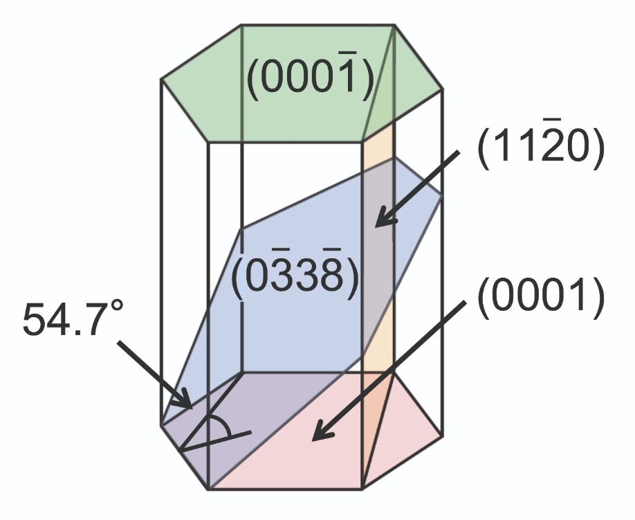
Figure 1. Major crystal faces in 4H-SiC. The (0338) face is located at an off-angle of 54.7 degrees from the (0001) face.
What’s needed is to replace silicon devices with those made from wide bandgap materials, such as SiC and GaN. This pair attract much attention because they have the upper hand over silicon on many fronts, including a higher dielectric breakdown electric field, a superior electron saturation velocity, and a greater thermal conductivity. Thanks to these characteristics, SiC and GaN provide a higher breakdown voltage and a reduced on-resistance, leading to lower conduction losses.A noteworthy difference between SiC and GaN is the quality of the crystal. Bulk SiC has fewer crystal defects, enabling the manufacture of high-quality SiC epitaxial substrates, and in turn the production of vertical SiC power devices. These devices, which use the whole surface of the epitaxial layer, combine a high current with a breakdown voltage of 600 V or more. Due to this, SiC is expected to have its greatest success in high-voltage applications that achieve high power, while GaN is expected to be used in low output power applications.
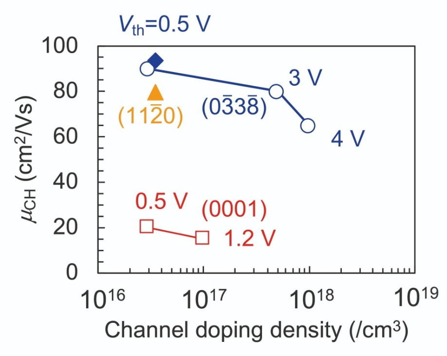
Figure 2. The doping density dependence of channel mobility of SiC lateral MOSFETs. The (0338) face shows a higher channel mobility and a higher threshold voltage than other crystal faces.
SiC devices will displace the silicon insulated-gate bipolar transistor (IGBT), which combines a high breakdown voltage with a low resistance. Due to this device’s bipolar operation, switching losses increase with the electron-hole recombination time. That’s not the case with the SiC MOSFET, a unipolar device that provides high-speed switching and a higher breakdown voltage.A great groove
At Sumitomo Electric Industries Ltd., Japan, we have developed a new architecture for the SiC MOSFET. It features V-groove trenches, enabling us to exploit a face with a higher mobility.
This development is able to draw on our vast experience surrounding the production of compound semiconductor products, which include GaN HEMTs, GaAs FETs and the substrates that form their foundation. More recently, we have been developing SiC crystals, and have gone on to start mass production of 6-inch SiC epitaxial substrates, which we refer to as EpiEra. They are produced using a high-quality, cost-effective growth technology – we have named this our multi-parameter and zone-controlled SiC growth technology. We use a unique simulation technique to determine the most appropriate doping concentration uniformity for realising the intended device performance and yield. Through vertical integration of our SiC material and device technologies, we produce SiC MOSFETs with a high performance and a high yield.
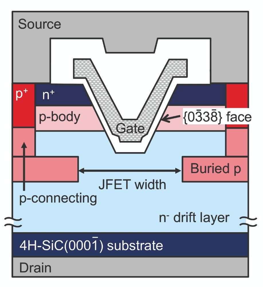
Figure 3. A cross-sectional view of a SiC VMOSFET.
We have developed our novel MOSFET architecture because the channel mobility in conventional designs is substantially lower than the bulk mobility, due to a high interface state density. To demonstrate what can be achieved, we fabricated a lateral MOSFET on 4H-SiC(0338) face, which is located at an off-angle of 54.7 degrees from the (0001) face (see Figure 1).Our results show that this is the best face for making SiC MOSFETs, because the channel mobility is highest for all doping concentrations, due to a lower interface state density and a higher free-electron ratio (see Figure 2). When employing a doping concentration of 1018/cm3, a high channel mobility of 60 cm2 V-1 s-1 is realised alongside a threshold voltage that is as high as 4 V – this is high enough to suppress erroneous ignition at high temperatures.
To exploit the benefits of this face, over the last few years we have developed and commercialised the 4H-SiC V-groove trench MOSFET, a device we refer to as a VMOSFET. Recently, efforts have been directed at high power conversion efficiency, so that the devices can handle hundreds of amps and have a breakdown voltage above 1 kV. These transistors feature 4H-SiC{0338} trench side walls that have a higher channel mobility than other SiC crystal faces (see Figure 3 for a diagram of this structure). Using this design, channel resistance can be reduced while realising a high channel density.
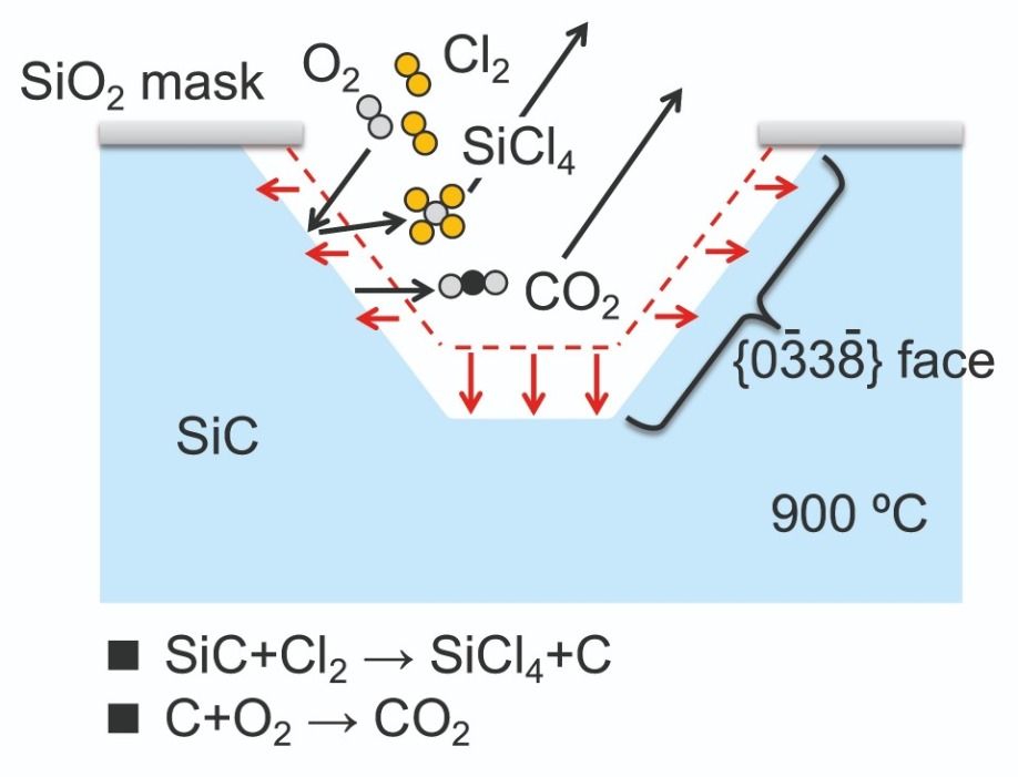
Figure 4. Chlorine etching creates the V-grooves of the MOSFET.
The key to producing this device is the use of a chemical etching process to form the V-groove trenches. We use silicon dioxide as the etching mask, with etching undertaken at around 900 °C in a chlorine ambient. During this process, chlorine produces a chemical change in the surface, with SiC converted to carbon, which then reacts with oxygen. The resultant silicon chloride and carbon dioxide vaporizes at a high temperature (see Figure 4).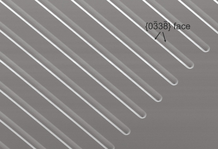
Figure 5. Scanning electron microscopy (SEM) image of a V-groove.
This process exposes {0338} faces, which are extremely stable. Note that with a conventional process to form U-shaped trenches, such as reactive-ion etching, this would lead to etching damage and the formation of sub-trenches. The high-quality of the faces produced by our process can be seen in the images of a scanning electron microscope (see Figure 5).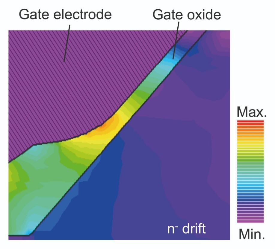
Figure 6. Electric field distribution around the V-groove trench bottom calculated by technology CAD for a lifetime estimation.
A shortcoming of the trench structure is that the gate oxide film that forms on the bottom of the trench breaks easily when a high voltage is applied to the device. When this happens, the electric field concentrates on the gate oxide film. To address this and enhance the reliability of the VMOSFET, we implant p-type electric-field-alleviating regions around the groove bottom. With this addition, the application of a high voltage to the drain electrode causes the electric field to concentrate on the buried p-region edge. Making this modification alleviates the electric field on the gate oxide film.
With this design, we are able to increase the switching speed and reduce switching loss by reducing the parasitic capacitance between the gate and drain electrodes. This is accomplished by creating a source potential, by electrically connecting the buried p-regions to the source electrode with p-connecting regions.
Proven reliability
To ensure a low on-resistance, and a low oxide electric field that leads to long-term reliability, it is crucial to optimise the JFET width and the width between the buried p-regions. Our efforts related to this include our investigation of the relationship between the oxide electric field and the lifetime under a drain bias condition.
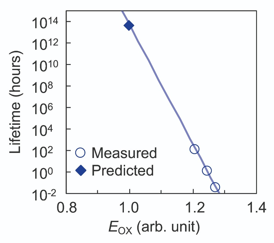
Figure 7. Long-term lifetime of VMOSFETs. Lifetime is estimated under a drain bias condition at Ta = 175 °C in the case of a 10 percent cumulative failure rate. The predicted lifetime is equal to 200 years under a 0.1 ppm cumulative failure-rate condition.
An estimate of the lifetime under a high-temperature reverse-bias condition has been obtained with test dies that have a dedicated structure. To increase the oxide electric field, dies with a V-groove gate trench structure have a large JFET width compared with the VMOSFETs designed for mass production. These tests have been conducted at an ambient temperature of 175 °C. The oxide electric field in these transistors has been calculated using Technology CAD simulation. Calculations of the electric field distribution reveal that the oxide electric field is highest on the bottom oxide edge, due to electric field crowding (see Figure 6). After we carried out the high-temperature reverse-bias tests, we analysed the damaged point of the VMOSFETs. We found that its location corresponded to our simulation’s highest point for the oxide electric field.Using these measurements, we have determined the impact of the oxide electric field on the lifetime. A plot for a 10 percent cumulative failure rate is shown in Figure 7.
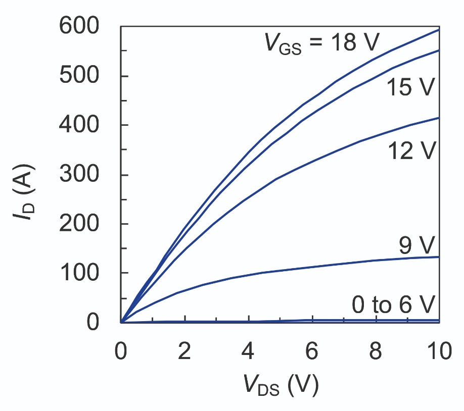
Figure 8. ID-VDS characteristics (VGS = 0 – 18 V) at Tj = 25 °C. The VMOSFETs exhibit a high current capability of 200 A DC and 600 A pulse.
For high-reliability applications, our target lifetime is more than 20 years for a 0.1 parts-per-million cumulative failure rate. We exceed this by a significant margin. For an oxide electric field of 1.0 – note that this is an arbitrary unit – the predicted lifetime is 4.5 x 10¹³ hours. That equates to a lifetime of 200 years under a 0.1 ppm cumulative failure rate condition, according to our calculations that relate the lifetime to the cumulative failure rate.Drawing on the high-temperature reverse-bias tests, we used simulations to design a structure that has a low on-resistance and an oxide electric field of 1.0 at a drain bias of 1200 V. This led us to fabricate VMOSFETs with an optimised design on a 150 mm wafer. Operating at a junction temperature of 25 °C, the resultant 6.0-mm-square die can handle a DC current of 200 A and pulses up to 600 A (see Figure 8). The specific on-resistance is just 3.1 mΩ cm2 for a gate-source voltage of 15 V and a drain-source voltage of 1 V; and at 25 °C, the threshold voltage is 4.6 V, for a drain-source voltage equal to the gate-source voltage, and a drain current density of 1 mA/mm2.
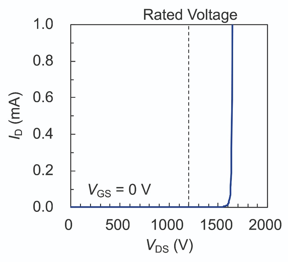
Figure 9. Blocking characteristics. The VMOSFETs show an adequate margin against a rated blocking voltage of 1200 V.
The breakdown voltage is well above the target, capable of withstanding up to 1640 V (see Figure 9). Another encouraging attribute is the small gate-to-drain capacitance – it is just 15 pF at a drain-source voltage of 800 V – enabling effective suppression of self-turn-on, due to the grounded buried p-regions that effectively block lines of electric force from the drain electrode.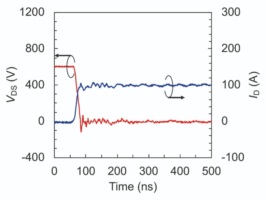
Figure 10. Fast switching characteristics of VMOSFETs under double pulse test. Conditions for this test are:
RG = 1.0 Ω, VGS = +15/-5 V, VDD = 600 V, ID = 100 A, L = 100 µH.
We have also performed a double pulse test with an inductive load, using a SiC Schottky barrier diode for the free-wheel device (see Figure 10 for details). This test highlights our VMOSFETs fast switching speed and low switching loss. Rise and fall times are 16 ns and 7 ns, respectively; and turn-on and turn-off energy loss are just 260 µJ and 270 µJ, making the total switching loss only 530 µJ.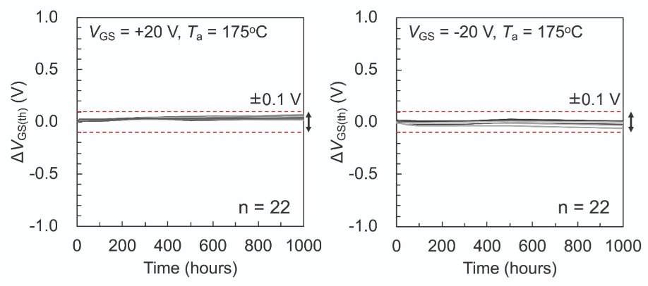
Figure 11. Stable threshold voltage of a VMOSFET under a high temperature gate bias test of VGS = +20 V (left) and -20 V (right) at Ta = 175 °C.
Further testing involved evaluating the threshold voltage stability of our VMOSFETs. Evaluation of 22 samples at 175 °C revealed threshold voltage shifts of less than 0.1 V after a 1000 hour high-temperature gate-bias test. This small shift is evidence of the stability and high quality of the gate oxide on {0338} crystal faces.
Our successful development of our 1200 V / 200 A VMOSFET has enabled us to expand our line-up for this class of transistor (see Table 1). From a user’s perspective, the adoption of VMOSFETs allows: better performance at both the component and system level; greater capability in designing far smaller components; and a stable supply chain and better quality management. We anticipate that the superior characteristics of our VMOSFETs, which combine low power loss and high reliability, will underpin further expansion in the SiC market.
A part of this R&D was carried out as one of the Super clean room Power Electronics Line (SPEL) joint research consortium activities hosted by the National Institute of Advanced Industrial Science and Technology.
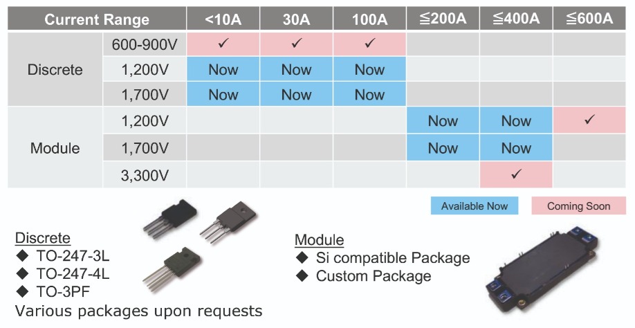
Table 1. Sumitomo Electric Industries’ line-up of VMOSFET products.
K. Wada et al. Mater. Sci. Forum 105-108 963 (2019)
T. Hiyoshi et al. Mater. Sci. Forum 740-742 506-509 (2013)
T. Hatakeyama et al. Appl. Phys. Express 12 021003 (2019)


