
Plug and play Characterization
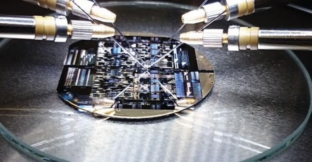
An integrated electrical test platform builds on the advantages of foundry services by offering chip-level test and characterization
BY Axel SchOEnau, Moritz Baier, Francisco Soares, Guillaume Binet, Norbert Grote, Jonas Hilt, Peter Hellwig, Ronald Freund AND Martin Schell FROM THE Fraunhofer Heinrich Hertz Institute
There are many applications for the InP PIC. It is already deployed in sensing, telecommunication, biophotonics and signal-processing – and it may not be long before it is used in quantum optics, LiDAR and AI. This technology has much appeal in all these applications, due to its low cost and the opportunity to slash the size compared with classical optics.
Manufacturing InP PICs involves several complex, costly processing steps. But this does not have to prohibit researchers at companies and universities from investigating this technology, thanks to the availability of photonic InP foundry services. By sharing wafer space with other customers, fabrication costs for a whole wafer can be distributed between the various parties (see Figure 1). Using a process design kit, each customer can place pre-defined building blocks of active and passive integrated components on the InP wafer according to the foundry’s design rules.
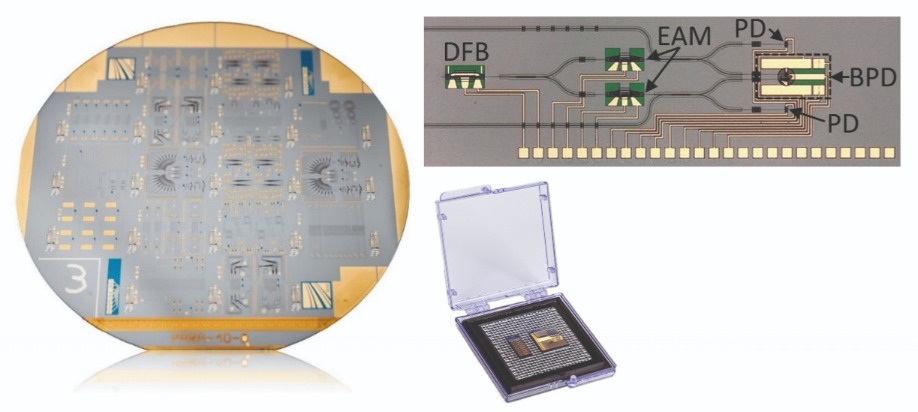
Figure 1. A 3-inch InP based multi-project wafer containing customers’ PIC designs and test structures (left). Single PIC with metal routing for on-chip DC characterization of balanced photodiodes (BPDs) (top right). This chip contains distributed feedback lasers (DFBs), electro-absorption modulators (EAMs) and photodiodes (PDs). Bare chips in a gel pack before shipping to the customer (bottom right).
Many of these building blocks have to be actively controlled. Current sources are needed to control light sources, such as distributed feedback lasers and distributed Bragg reflector lasers, and also gain sections, thermal optical phase shifters and heaters.In addition, there is a need for voltage sources, used to control electro-absorption modulators and photodiodes. PICs also feature appropriate metal routing, to facilitate probing and simplify wire bonding to either electronics or an interposer board.
If a customer does not require packaging, bare InP PICs are shipped to the customer in a gel pack (see Figure 1). On arrival, the customer has to undertake experimental verification of the prototype. That’s not easy, as it requires measurement equipment with a total price tag of several hundred thousand euros or more, and experience in handling PICs, to prevent them from damage.
To overcome these daunting obstacles, our team at the Fraunhofer Heinrich Hertz Institute has developed an integrated test platform for generic PICs. Our work builds on the InP PIC foundry services that we offer. Those working in this industry now have the opportunity to access foundry services that are no longer restricted to epiwafer growth and processing, but extend to test and characterization.
Conventional PIC measurements
One of the expenses for engineers carrying out their own PIC testing is the purchase of a temperature-controlled chuck. It is needed to house the PIC and provide mechanical stabilisation, which can be realised with a vacuum. Further expense may be incurred to couple a fibre to the PIC. If that’s required, equipment is needed for coarse and fine alignment. A translation stage for each fibre ensures coarse alignment to the waveguides or on-chip spot size converters, while fine alignment can be realised with piezo motors with sub-micron step sizes. An example of a PIC measurement set-up is illustrated in Figure 2.
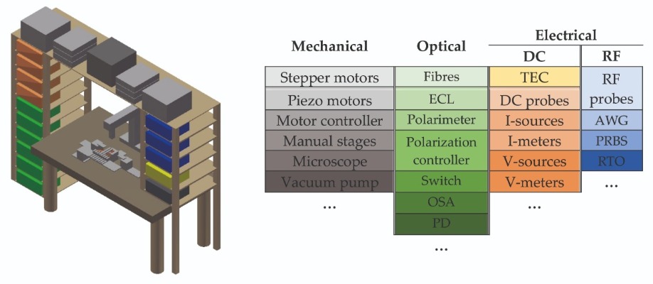
Figure 2. Schematic of a conventional PIC measurement set-up (left). Listed mechanical, optical and electrical systems (right).
A popular choice for the input light source for the PIC is an external cavity laser. It provides well controlled wavelengths and powers. Experimental set-ups also tend to include optical switches, used to direct out-coupled light to detection and analysis instruments, such as optical spectrum analysers and photodetectors. As testing may also involve electrical biasing and sweeps, there is the need for current and voltage sources, in combination with corresponding meters. To apply these currents and voltages to PIC building blocks, researchers often use probe needles (see Figure 3).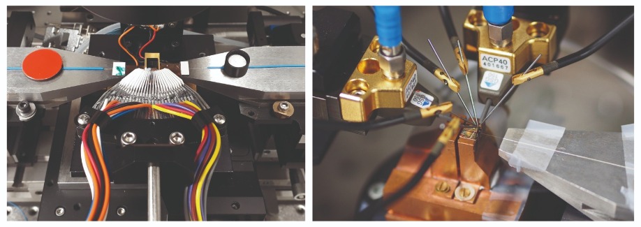
Figure 3. Electrical probing of a PIC with a 26 needle DC multiprobe (left), RF probes and single needles contacting a PIC (right, image courtesy of Weiming Yao, Department of Electrical Engineering, Photonic Integration, TU Eindhoven).
Measurements of data transmission require additional equipment, such as arbitrary waveform generators, pseudo-random bit stream sources and real-time oscilloscopes. If high-frequency measurements are to be made, RF-probes have to be placed on the PIC besides biasing needles. That’s tricky, requiring many probes to be positioned on a chip that is smaller than a finger nail.Simplifying evaluation
Given all these challenges associated with evaluating a PIC, affordable plug-and-play characterization is highly desirable. We are giving this to our customers with our new PIC evaluation set-up, which we have named PIConnect. By featuring integrated laser drivers and general purpose current and voltage sources, it enables parallel operation of PIC building blocks. Researchers investing in a PIConnect receive a mainboard, which contains all sources plus a plugged-in micro-controller board, as well as a PIC Board on a cooling stack to assemble the PIC (see Figure 4).

Figure 4. PIConnect comprised of mainboard (that has 8 current sources, 8 voltage sources, 4 laser drivers (Thorlabs MLD203P1) and one temperature controller (Thorlabs MTD415T)) with a microcontroller board (SAME70 XPLAINED) and PIC Board integrated in an existing measurement set-up (left). Photograph of the PIC assembled on the PIC Board with a Peltier element and mechanical mounting plate (centre). Fibre coupling is undertaken using tapered fibres and piezo actuators. Glued and wire-bonded PIC on a PIC Board (top right) and pinout of the PIC Board bond pads (bottom right; shows only exemplary wire bonding). The pitch between two adjacent pads is 200 µm.
The mainboard contains eight current sources, eight voltage sources, four laser drivers, and one temperature controller that supports a 10 kΩ thermistor temperature sensor. The temperature controller drives currents up to ±1.5 A.Each of the current sources provides an output current of up to 200 mA at up to 5 V. Voltage monitoring is integrated. For the voltage sources, the output can be adjusted between -10 ... +10 V. The current, which has integrated monitoring, cannot exceed 20 mA. Laser drivers can deliver currents up to 200 mA at a maximum voltage of 3 V. For this first-generation product, all measurements are made with 12-bit resolution.
To evaluate the PIC, it has to be mounted on the PIC Board and bonded to equally spaced pads. Connecting the PIC Board to the mainboard is done by a flexible flat cable containing 50 wires. The PIC Board is positioned on a cooling stack with a 20 mm by 20 mm Peltier element that enables precise temperature controlling through a 10 kΩ thermistor. Within this set up, the Peltier element is directly connected to the thermo-electric controller on the mainboard (see Table 1 for details of the hardware specifications).

Table 1. Components of the mainboard with specifications and pinout.
To access the information generated by PIConnect, it is connected to a PC via Ethernet using a web interface. A Python-based graphical interface enables the setting of constant currents and voltages, and applying sweeps within defined ranges (see Figure 5).We recommend using predefined Python written functions when embedding PIConnect into an existing measurement set-up. Adopting Python’s Application Programmable Interfaces equips the user with complete control of automated measurements in the kilohertz-regime – the only limit is the web interface speed.
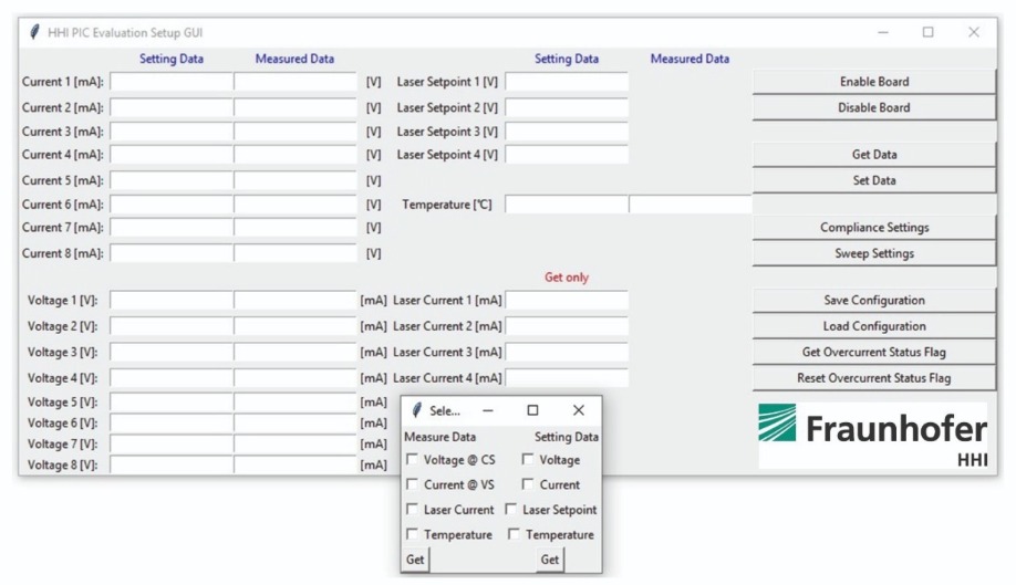
Figure 5. Python-based graphical user interface for setting and getting measurement parameters. Single sweeps, saving and loading are also possible.
Demonstrating capabilityTo demonstrate the capability of our PIConnect, PIC Board and mainboard are introduced to our existing PIC measurement set-up, which is shown in Figure 4. We use a polarimeter PIC as our showcase device under test. This chip has a Mach-Zehnder based structure, which uniquely maps measured photocurrents to the corresponding input polarization of the light. The polarimeter PIC works for wavelengths across the entire C-band and beyond, but here it is demonstrated at just 1530 nm. We presented the details of this PIC at OFC 2019.

Figure 6. Integrated polarimeter PIC. Light is coupled from a fibre into one of the input ports on the left side. Five on-chip photodetectors (PDs) measure the photocurrents, and five thermal-optic phase shifters (TOPS) tune the configuration. The PIC further consists of polarization rotators (PR) and multimode interferometers (MMI).
During this test we launched 595 distinct polarizations across the Poincaré sphere into the polarimeter. The polarization states of the light are recorded using blue circles (see Figure 7). For this measurement, five integrated photodetectors are biased at -2 V, and at each polarization the photocurrents are recorded by PIConnect.This test platform produces a mean mapping accuracy of around 1.8°. This low value highlights the competitive performance of PIConnect. We will offer PIConnect as an additional service to our customers. We know that they will welcome its introduction, as it is more than ten times more cost effective than the laboratory equipment normally used for PIC characterization, such as the combination of multiple dual-channel source meters, a Peltier controller and probing mechanics.
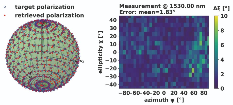
Figure 7. Experimental results at a wavelength of 1530 nm using PIConnect. On the left is a Poincaré sphere, 595 target (blue circles) and retrieved (red dots) polarizations are visualised. The corresponding heatmap on the right shows the measurement accuracy Dx of the PIC. Dx gives the angular measurement error on the Poincaré sphere. For this measurement the average is 1.83°.
Note that it is possible to use two or more mainboards in parallel. This offers a straightforward approach to scaling the number of laser drivers, and current and voltage sources. To adopt this approach, the PIC Board must be re-designed so that it can connect several flat cables.We are continuing to work on simplifying PIC characterization. Through our involvement in the EU Horizon 2020 project InPulse – short for Indium-Phosphide Pilot Line for up-scaled, low-barrier, self-sustained, PIC ecosystem – we are working on automated, standardised routines to characterise PICs. The test platform will be exploited to offer a rigid, predictable and reproducible verification mechanism for process design kit contents and customer designs.
Together with the joint European platform for photonic integrated components and circuits (JePPIX), we will be offering PIConnect as an additional option to the customers of multi-project wafer runs. Our next step, enabled by general PIC design rules, is to make PIConnect available to customers using other foundries. A longer term goal is to integrate optical coupling and RF feeds, to improve the functionality of PIConnect. Through our efforts, lower-cost, simpler options for testing InP PICs are going to be available to more players within this industry – and that will help to grow the market for this technology.
M. Smit et al. APL Photonics 4 050901 (2019)
https://www.hhi.fraunhofer.de/en/departments/pc/research-groups/photonic-inp-foundry.html
M. Baier et al. Appl. Sci. 9 2987 (2019)
M. Baier et al. “Fully Integrated Stokes Vector Receiver for 400 Gbit/s,” in Optical Fiber Communication Conference (OFC) 2019, OSA Technical Digest (Optical Society of America, 2019), paper Tu3E.2.
https://cordis.europa.eu/project/id/824980


