Loading...
News Article

Laytec tool plays key role in VCSEL research

News

EpiCurve TT metrology helps reveal and control AlInN strain and alloy compositions

Last year, scientists from Meijo University and the R&D division of Stanley Electric in Japan demonstrated high-efficiency and high-power operation for blue GaN-based VCSELs with AlInN /GaN distributed Bragg reflectors (DBRs). They published the results in Applied Science.

These AlInN /GaN DBRs are used at the front (emitting) side of the VCSEL that emits through the GaN substrate and is completed by a second, dielectric DBR at the VCSEL’s back-side. Hence, perfect lattice match of the AlInN in the front DBR is essential for enabling extremely low-defect InGaN layers in the active zone of the device that is grown on top of the AlInN /GaN DBRs.

Now, the German metrology company Laytec has reported that a paper in the Journal of Crystal Growth by scientists from Meijo University shows the power of its EpiCurve TT metrology tool in revealing and controlling the AlInN strain and alloy compositions at accuracy levels of XRD already during growth of the epitaxial layers.

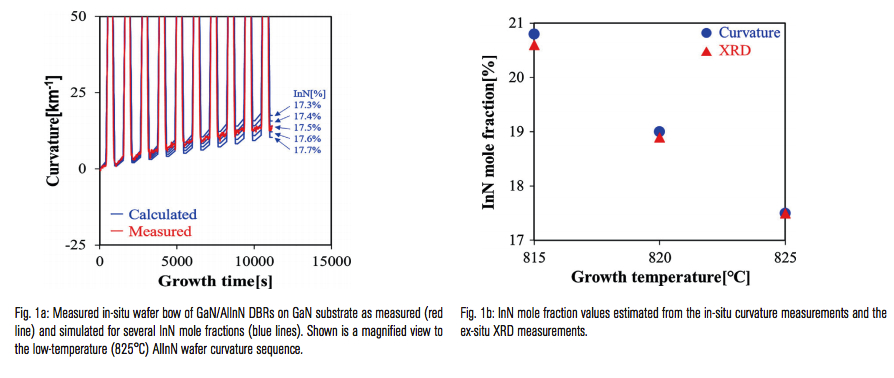
The team developed a model for in-situ wafer curvature values of AlInN/GaN distributed Bragg reflectors (DBRs) and determined InN mole fractions in the DBRs with the model. In order to develop the model, they experimentally investigated contributions of substrate temperature ramping and a GaN growth to changes in the in-situ curvature values during the AlInN/GaN DBR growth.

They found that an increase of curvature changes at the substrate temperature ramping steps was explained by an increase of the total epitaxial layer thicknesses. Another finding was that strain in the GaN layers at the GaN layer growth steps was almost zero. Finally, they determined the InN mole fractions in the AlInN layers by using the model, showing excellent agreements with the values estimated from ex-situ X-ray diffraction measurements. The model reveals not only the entire in-situ curvature change profile but also the InN mole fraction under the precisely lattice-matched condition of AlInN/GaN DBRs.


'High-Power GaN-Based Vertical-Cavity Surface-Emitting Lasers with AlInN/GaN Distributed Bragg Reflectors' by Masaru Kuramoto et al; Appl. Sci. 2019, 9(3), 416

'In-situ curvature measurements of AlInN/GaN distributed Bragg reflectors during growths containing substrate temperature ramping steps' by Kei Hiraiwa et al; Journal of Crystal Growth Volume 531, 1 February 2020
SiC MOSFETs: Understanding the benefits of plasma nitridation
Wolfspeed reports Q2 results
VueReal secures $40.5m to scale MicroSolid printing
Mitsubishi joins Horizon Europe's FLAGCHIP project
Vishay launches new high voltage SiC diodes
UK team leads diamond-FET breakthrough
GaN adoption at tipping point, says Infineon
BluGlass files tuneable GaN laser patents
QD company Quantum Science expands into new facility
Innoscience files lawsuit against Infineon
Riber revenues up 5% to €41.2m
Forvia Hella to use CoolSiC for next generation charging
Photon Design to exhibit QD simulation tool
Ortel transfers CW laser fabrication to Canada
Luminus adds red and blue multi-mode Lasers
PseudolithIC raises $6M for heterogeneous chiplet tech
Mesa sidewall design improves HV DUV LEDs
IQE revenue to exceed expectations
'Game-changing' VCSEL system targets clinical imaging
German start-up secures finance for SiC processing tech
Macom signs preliminaries for CHIPS Act funding
IQE and Quintessent partner on QD lasers for AI
EU funds perovskite tandems for fuel-free space propulsion
EU to invest €3m in GeSi quantum project
Transforming the current density of AlN Schottky barrier diodes
Turbocharging the GaN MOSFET with a HfO₂ gate
Wolfspeed launches Gen 4 SiC MOSFET technology
Report predicts high growth for UK's North East
Element Six unveils Cu-diamond composite
SemiQ launches hi-rel 1700V SiC MOSFETs
Lynred to exhibit Eyesential SWIR sensor for machine vision
Thorlabs buys VCSEL firm Praevium Research
×
Search the news archive

To close this popup you can press escape or click the close icon.
Logo
x
Logo
×
Register - Step 1

You may choose to subscribe to the Compound Semiconductor Magazine, the Compound Semiconductor Newsletter, or both. You may also request additional information if required, before submitting your application.


Please subscribe me to:


You chose the industry type of "Other"

Please enter the industry that you work in:
 
x
Adblocker Detected
Please consider unblocking adverts on this website