
High-quality BN grown at atmospheric pressure
Graphene Flagship researchers produce large and very high-quality crystals at room temperature
Graphene Flagship researchers at RWTH Aachen University, Germany and ONERA-CNRS, France, in collaboration with researchers at the Peter Grunberg Institute, Germany, the University of Versailles, France, and Kansas State University, US, have reported a significant step forward in growing monoisotopic hexagonal boron nitride at atmospheric pressure for the production of large and very high-quality crystals.
The 2D compound semiconductor hexagonal boron nitride (hBN) is the unsung hero of graphene-based devices. Much progress over the last decade was enabled by the realisation that 'sandwiching' graphene between two hBN crystals can significantly improve the quality and performance of the resulting devices. This finding paved the way to a series of exciting developments, including the discoveries of exotic effects such as magic-angle superconductivity and proof-of-concept demonstrations of sensors with unrivalled sensitivity.
Until now, the most widely used hBN crystals came from the National Institute of Material Science in Tsukuba, Japan. These crystals are grown using a process at high temperatures (over 1500degC) and extremely high pressures (over 40,000 times atmospheric pressure). "The pioneering contribution by the Japanese researchers Taniguchi and Watanabe to graphene research is invaluable", says Christoph Stampfer from Graphene Flagship Partner RWTH Aachen University, Germany. "They provide hundreds of labs around the world with ultra-pure hBN at no charge. Without their contribution, a lot of what we are doing today would not be possible."
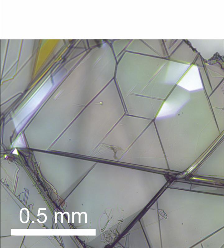
However, this hBN growth method comes with some limitations. Among them is the small crystal size, which is limited to a few 100 μm, and the complexity of the growth process. This is suitable for fundamental research, but beyond this, a method with better scalability is needed. Now Graphene Flagship researchers tested hBN crystals grown with a new methodology that works at atmospheric pressure, developed by a team of researchers led by James Edgar at Kansas State University, US. This new approach shows great promise for more demanding research and production.
"I was very excited when Edgar proposed that we test the quality of his hBN", says Stampfer. "His growth method could be suitable for large-scale production". The method for growing hBN at atmospheric pressure is indeed much simpler and cheaper than previous alternatives and allows for the isotopic concentration to be controlled.
"The hBN crystals we received were the largest I have ever seen, and they were all based either on isotopically pure boron-10 or boron-11" says Jens Sonntag, a graduate student at Graphene Flagship Partner RWTH Aachen University. Sonntag tested the quality of the flakes first using confocal Raman spectroscopy. In addition, Graphene Flagship partners in ONERA-CNRS, France, led by Annick Loiseau, carried out advanced luminescence measurements. Both measurements indicated high isotope purity and high crystal quality.
However, the strongest evidence for the high hBN quality came from transport measurements performed on devices containing graphene sandwiched between monoisotopic hBN. They showed equivalent performance to a state-of-the-art device based on hBN from Japan, with better performance in some areas.
"This is a clear indication of the extremely high quality of these hBN crystals," says Stampfer. "This is great news for the whole graphene community, because it shows that it is, in principle, possible to produce high quality hBN on a large scale, bringing us one step closer to real applications based on high-performance graphene electronics and optoelectronics. Furthermore, the possibility of controlling the isotopic concentration of the crystals opens the door to experiments that were not possible before."
Mar García-Hernández, work package leader for enabling materials, adds: "Free-standing graphene, being the thinnest material known, exhibits a large surface area and, therefore, is extremely sensitive to its surrounding environment, which, in turn, results in substantial degradation of its exceptional properties. However, there is a clear strategy to avoid these deleterious effects: encapsulating graphene between two protective layers."
García-Hernández continues: "When graphene is encapsulated by hBN, it reveals its intrinsic properties. This makes hBN an essential material to integrate graphene into current technologies and demonstrates the importance of devising new scalable synthetic routes for large-scale hBN production. This work not only provides a new and simpler path to produce high-quality hBN crystals on a large scale, but it also enables the production of monoisotopic material, which further reduces the degradation of graphene when encapsulated by two layers."
Andrea C. Ferrari, science and technology officer of the Graphene Flagship and chair of its management panel, adds: "This is a nice example of collaboration between the EU and the US, which we fostered via numerous bilateral workshops. Devising alternative approaches to produce high-quality hBN crystals is crucial to enable us to exploit the ultimate properties of graphene in opto-electronics applications. Furthermore, this work will lead to significant progress in fundamental research."


