
Scientists learn more about SiC defects
Study pinpoints the atomistic mechanisms responsible for extended defect generation and evolution
Silicon wafers of high purity (99 percent or higher) single-crystalline material can be obtained via a combination of liquid growth methods, such as pulling a seed crystal from the melt and by subsequent epitaxy. The catch is that the former process can't be used for the growth of SiC, because it lacks a melting phase.
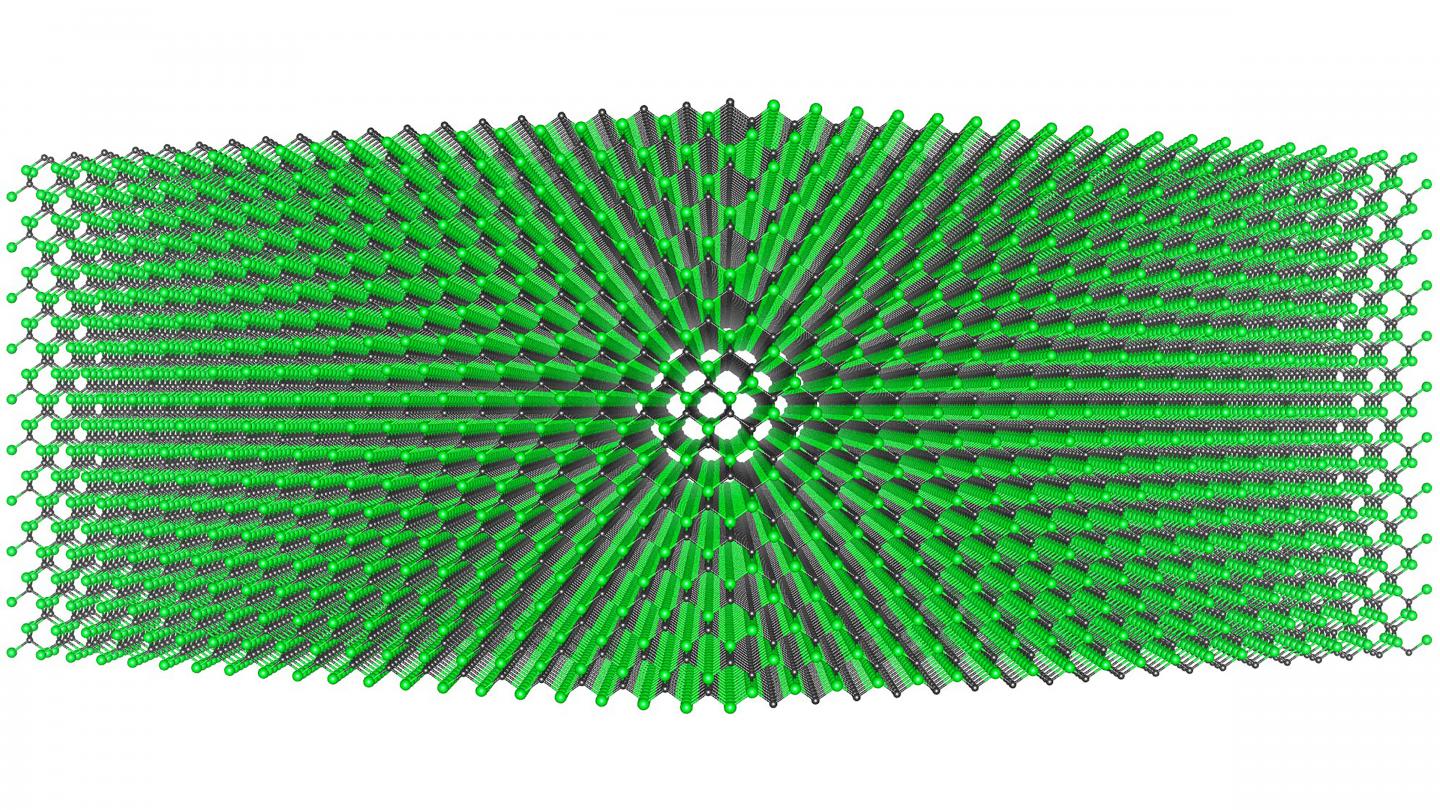
In the journal Applied Physics Reviews, Giuseppe Fisicaro from the Consiglio Nazionale delle Ricerche, Istituto per la Microelettronica e Microsistemi (CNR-IMM) in Italy, and an international team of researchers, led by Antonio La Magna (Novasic, France), describe a study of the atomic mechanisms governing extended defect kinetics in cubic SiC (3C-SiC), which has a diamond-like zincblende (ZnS) crystal structure that manifests both stacking and anti-phase instabilities.
"Development of a technological framework for the control of crystalline imperfections within SiC for wide bandgap applications can be a game-changing strategy," said Fisicaro.
The researchers' study pinpoints the atomistic mechanisms responsible for extended defect generation and evolution.
"Anti-phase boundaries - planar crystallographic defects representing the contact boundary between two crystal regions with switched bonds (C-Si instead of Si-C) - are a critical source of other extended defects in a plethora of configurations," he said.
Eventual reduction of these anti-phase boundaries "is particularly important to achieve good-quality crystals that can be used in electronic devices and enable viable commercial yields," said Fisicaro.
So they developed an innovative simulation Monte Carlo code based on a superlattice, which is a spatial lattice that contains both the perfect SiC crystal and all crystal imperfections. It helped "shed light on the various mechanisms of defect-defect interactions and their impact on the electronic properties of this material," he said.
Emerging wide bandgap semiconductor devices like SiC have the potential to revolutionise the power electronics industry and bring huge environmental benefits. "If the world's silicon power devices used within this range with were replaced by 3C-SiC devices, a reduction of 1.2x10¹⁰ kilowatts per year could be obtained," Fisicaro said.
"This corresponds to a reduction of 6 million tons of carbon dioxide emissions," he said.
The researchers concluded that the low cost of the 3C-SiC hetero-epitaxial approach and the scalability of this process to 300-mm wafers and beyond make this technology extremely competitive for motor drives of electric or hybrid vehicles, air conditioning systems, refrigerators, and LED lighting systems.
This work is part of the European Union's Horizon 2020 CHALLENGE Program; HORIZON 2020-NMBP-720827).
'Genesis and evolution of extended defects: The role of evolving interface instabilities in cubic SiC' by Giuseppe Fisicaro et al; Applied Physics Reviews, April 28, 2020


