
A knowledgeable, responsive partner for plasma technologies
Shipments of Oxford Instruments Plasma Technology’s deposition and etch tools are rising, due to their deployment in critical processes used for chip manufacture in growing markets
BY RICHARD STEVENSON
HAS THERE EVER BEEN a better time to be working within the compound semiconductor industry? Never before have there been so many emerging markets tipped to generate billions and billions of dollars in device sales. Over the next few years shipments of GaN transistors will underpin the roll-out of 5G infrastructure; SiC transistors and diodes will enhance electric vehicles; GaAs VCSELs will become more common in smartphones and provide a source for other 3D sensing applications; and interest will mushroom in photonic integrated circuits, which can be used for communication and sensing.
All this activity is particularly good news for the makers of processing equipment for the compound semiconductor industry. That includes Oxford Instruments Plasma Technology, a division of Oxford Instruments based in Yatton, just outside Bristol.
According to Managing Director of Plasma Technology, Mike Gansser-Potts, the compound semiconductor market is now entering a high-volume manufacturing phase where the performance it enables is demanded by global trends, such as efficient energy and driverless vehicles.
Plasma Technology is in a particularly strong position to make the most of these opportunities, because it has been supporting its customers on the research and development of these devices for almost forty years.
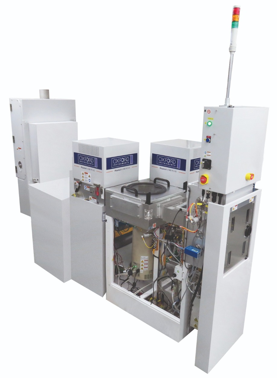
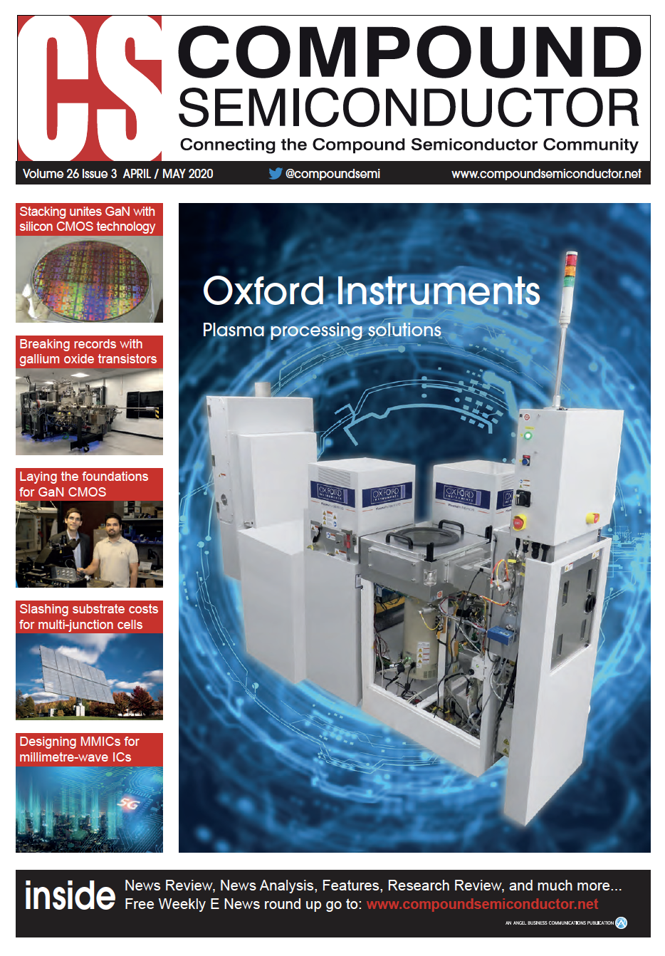
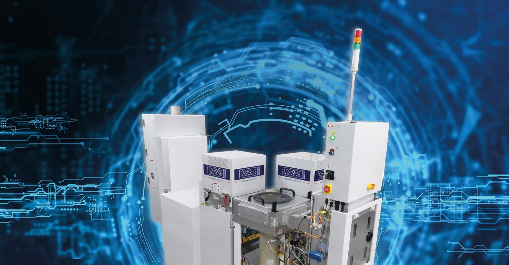
Atomfab is a newly released product that sets a new benchmark for plasma-enhanced, atomic-layer deposition.
“We have already had success with customers, VCSEL manufacturers for example, transitioning from corporate R&D into high-volume manufacturing,” says Gansser-Potts. “We achieve this by truly understanding the customer’s devices and how our systems can enhance the performance of these devices.”
The strategy of Plasma Technology is to focus on critical layers and steps within the device process flow, where it has a deep understanding and can bring value. It can increase device performance, while bringing down the cost of the wafers, says Gansser-Potts. “We have major investment across the company to achieve this.”
Some of the companies that Gansser-Potts and his colleagues are working with are device makers that are in the late research stage, or in the corporate research stage. For these firms, Plasma Technology is accompanying them on their journey to production. When they succeed, Plasma Technology’s tools are qualified before the chipmaker enters high-volume production.
Working with a client in this manner is beneficial on two fronts says Vice-President of Strategic Production Markets, Brian Dlugosch. He points out that it brings in revenue from the outset, and it leads to sales during the manufacturing phase. “That allows you to make money with your equipment for a longer period of time.”
Plasma Technology is also well-positioned to assist in the R&D sector, where the company has held a strong position for decades. Today it is showing no signs of complacency, having recently appointed a market specialist to oversee its activities in that area. Staff are also being recruited to support the production side of the business, where there has been the launch of new software and hardware.
“We have just launched Atomfab, for example, which is much faster than any product we have produced before for atomic layer deposition,” says Gansser-Potts. “And we are just launching PTIQ, which is our control software that is much more tailored to a production environment.”
With so many market opportunities available right now, it is critical to direct efforts at the ones offering the best chances of success. “If we try and spread the net too wide, we will have a small amount of many different markets,” reasons Gansser-Potts, who has adopted and led a well-defined strategy: focusing on really critical processes where Plasma Technology has a competitive advantage and a relationship with the developing client base.
A plasma portfolio
By offering a portfolio of tools, the engineers at Plasma Technology can help customers to find the most suitable one for their needs. For example, if device makers need to etch AlGaN, they can choose between equipment that provides an inductively coupled plasma etch and that producing an atomic layer etch.
In addition, customers may choose to buy several tools, each carrying out a different step in the production process. One obvious benefit is that the fab has to deal with fewer tool suppliers. But that’s not the only gain – it also allows the use of a cluster system, which can improve the quality of the interface between the oxide and the semiconductor, by avoiding vacuum breaks between process steps.
Rewind the clock a few years and many customers would buy tools, shut the door and rarely communicate with their supplier. Today, however, that’s not the norm – many chipmakers now want assistance and support. “We see customers that are in corporate R&D that are willing to pay big service contracts, saying yes we want maintenance, yes we want spare parts,” explains Mark Dineen, Technical Marketing Manager at Plasma Technology.
It’s a change that reflects the gradual shifting of the compound semiconductor industry towards the working practices of the more mature, more open silicon industry. There, market strength is reached by helping customers to increase the number of good wafers produced each day, while lowering the cost. The chipmakers in the silicon industry are not concerned by the appearance of the tool. Klaas Wisniewski, Strategic Business Development Director, hopes that the compound semiconductor industry moves in the same direction, placing value on how Plasma Technology can help to lower cost, increase throughput and enable device functionality.
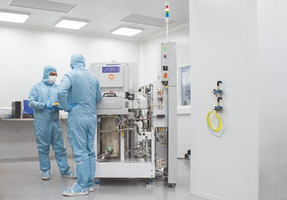
Oxford Instruments hasdeveloped new processing solutions in its fully equipped lab in Yatton, UK.
Efforts on all these fronts are supported by the work in the Application Lab. In the last decade, the company has made much investment in this, installing 25 process chambers at their main facility, and another seven at a facility in Taiwan. Using these chambers, Plasma Technology’s engineers undertake marathon runs and see if there are any changes to process or material characteristics. This allows the company’s technical team to advise on when it is necessary to clean a tool, and how far a particular parameter can shift before it changes the material properties. Assessments are made with a suite of characterisation techniques that include ellipsometry, atomic force microscopy, scanning electron microscopy and confocal microscopy. A Raman spectrometer is being installed. To obtain device results, Plasma Technology collaborates with companies and universities.
Supporting customers
If firms that have invested in Plasma Technology’s tools run in to problems, engineers can pay a visit and help find a solution. When an emergency occurs, responses are quick wherever the customer may be, thanks to qualified engineers located at seven sites – one is in China, another in Japan, and there are also those in the US, Germany, Singapore, Taiwan and the UK. However, these days, thanks to remote access of data from tools, often all that’s needed is a ‘phone call.
“We have seen a huge growth in remote access to our equipment, so there is less need for hands-on,” explains Dean Furlong, Engineering and Global Services Director. “Two years ago we had pretty much zero remote access. We are now doing thousands and thousands of hours every month of remote support with our customers, whether that is advice, support or improvements.”
This is a significant change, as in years gone by, most chipmakers would have never shared any of their data with equipment manufacturers.
“We are trusted, and trusted significantly, but I don’t think it’s about us,” says Furlong. “It’s about a change in understanding the way the technology works.” A protected environment provides data transmission up to the cloud. For some device manufacturers, a willingness to share data also reflects a narrowing of their view in what is proprietary.
While some customers will welcome a closer relationship with a toolmaker, there are others that prefer to get on by themselves – at least, until there is a problem they can’t fix! For firms with that philosophy, Plasma Technology offers self-sufficiency packages. Once the chipmaker has bought the tool, its engineers are trained and certified on that equipment, so that they can manage themselves and utilise the software. However, if problems arise that they are unable to address, they can access immediate support by phone, and if necessary, have a visit from a Plasma Technology engineer, all as part of the package agreement.
There are an increasing number of products to help customers in the fabs with diagnostics and support assistance. “We have something called LiveAssist, which enables us to have real-time connectivity to site, giving augmented reality support,” says Furlong. Another improvement is the launch of the latest version of the company’s software platform. “Within that there are modules on the roadmap for analytics and diagnostic suites, which will give further enhanced capabilities, not just for ourselves, but for our customers, in terms of understanding what is happening in their environment, and being able to do predictive analytics in tool behaviour.”
“That predictive software is important because people don’t want to operate in a run-to-fail mode,” says Dlugosch. Instead of using a component to the end of its lifetime, engineers are now changing it at an earlier stage so that they can maintain production.
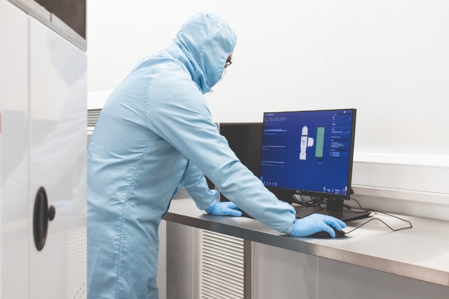
A new software control solution delivers enhanced experience in a production environment.
Deposition developments
At the SemiCon West exhibition last July, Plasma Technology added to its portfolio of atomic scale processing systems with the launch of AtomFab. It provides atomic layer deposition, and is designed to cater for the needs of makers of GaN power and RF devices.
“It really builds on our expertise on controlling the interfaces and ensuring that plasma processing is low damage, but also delivers high-quality and high throughput,” says Aileen O’Mahony, Product Manager, Atomic Scale Etching.
Dineen says that the introduction of AtomFab has gone extremely well, including the process transfer from the R&D platform to the high-volume manufacturing platform. “We maintained process performance at the device level while reducing the manufacturing cost per wafer for this process step by 75 percent.” The company secured its first high-volume manufacturing production order five months after the product launch.
There have also been successful customer demonstrations provided at Plasma Technology’s site, and interest from chipmakers working with other devices that have concerns related to plasma and substrate damage.
During the development of the AtomFab, engineers at Plasma Technology engaged with customers that would consider using this tool for development or production, in order to understand their priorities. “That’s really key, because we need to understand what they are working towards, because that will define the features,” says O’Mahony. The team also wanted to discover what features the customer didn’t value, to avoid including unnecessary capabilities.
While some device manufacturers will be keen to buy a new tool, others will want to upgrade what they already have. That’s possible, as detection systems and new software can be added to existing equipment to enhance its capabilities. However, some tools are now well off the pace – they can date back as far as the early 1980s – and if that’s the case, it’s more prudent to invest in state-of-the-art equipment.
Enhanced etching
For many years, Plasma Technology has offered tools for inductively coupled etching. Very recently, they have been complemented with equipment that can remove material by one atomic layer at a time. Together, these two etching techniques are ideal for the production of normally off AlGaN HEMTs, which have very thin layers, and a two-dimensional electron gas that must not be damaged. Inductively coupled etching can remove most material in good time, before atomic layer etching carefully takes away the last few atomic layers with great accuracy.
As the compound semiconductor industry has evolved, a growing number of device makers are having more stringent requirements related to the geometry of the processed wafer and the yield. This reflects the greater complexity of the design of many of today’s devices.
“If you take a HB LED, you can get away with a lot more, because it’s a larger area,” says Rob Gunn, Senior Product Manager. With a microLED, the sidewalls have a far greater influence over device performance, so there is more concern related to their quality. Having worked with microLED pioneers from their development days, Plasma Technology is well placed to have tools and processes for high-volume production of these devices.
Global goals
Given the capability of Plasma Technology’s tools to process SiC and GaN materials, it’s of no surprise that it is keen to have a strong presence in the Japanese market, where there is the likes of Fujitsu, Sumitomo, Sony and Nichia. But winning sales is far from easy. “The Japanese market is very, very demanding, and it’s culturally probably very challenging for the Western World,” says Wisniewski. So to try and get around these obstacles, Plasma Technology is working with a Japanese process partner, Ulvac. “We have a commercial agreement with them to help us commercialise our technology in the Japanese market.”
China may be best known for its highly competitive LED manufacture that has led to the commoditisation of this device. However, it is also active in other sectors of the compound semiconductor industry, where there are more promising opportunities for Plasma Technology. Right now, the Chinese government is working on the draft of its next five-year plan, which includes the classification of compound semiconductor materials under the third generation of semiconductors. “So it’s big exposure into SiC, where we have qualified processes,” say Wisniewski, who can also see a growth in activity in GaN RF, GaAs optoelectronics and microLEDs – all areas where Plasma Technology has great strength in critical processes.
For makers of these devices in China and beyond, Plasma Technology is a valued partner. For almost forty years it’s been looking after its customers by developing and refining hardware and associated critical processes – fulfilling their wishes is in its DNA.


