

AFRL: Breaking records with gallium oxide

Engineers at the US Air Force Research Laboratory are propelling the performance of gallium oxide devices to new highs, by realising record-breaking critical field strengths and making the first FETs with switching losses below those for silicon
BY RICHARD STEVENSON
If you have to begin from scratch, it’s very hard to develop a device with a new material. Efforts may have to begin by learning how to grow the crystals that are large enough to be sliced into native substrates. Much research may also be needed to work out how to deposit epilayers, make devices, test them, and then refine the processes. All this requires funding and a team of researchers with the right expertise to define an application space. Given all these challenges, it’s no surprise that progress on making devices with a new material is far from immediate, with some groups only entering the field when they can draw on the success of others.
That’s certainly the case with gallium oxide. Its attractive credentials have been known for many years – it is a material with an incredibly wide bandgap that indicates that it should make devices that are great for power switching – but it is only in the last decade that impressive device results have started to emerge from a few groups.
Laying the foundations for all the recent progress are materials scientists in Japan and Germany that developed processes to grow gallium oxide crystals from the melt and deposit epitaxial layers onto this foundation. The first application for gallium oxide was its use as a transparent conductive oxide substrate for GaN LED applications. But then researchers in Japan also made another important breakthrough – in 2012, a team at NICT, Japan, published experimental results showing a high breakdown voltage in gallium oxide devices made from the β-phase of the material.
One group that has noted NICT’s success and gone on to break records by partnering with some material suppliers is a team from the Air Force Research Laboratory (AFRL) at the Wright-Patterson Air Force Base in Ohio. Viewing gallium oxide as a very promising candidate for fast, low-loss power switching, they have attracted much attention by: setting a new benchmark for the critical field strength of gallium oxide FETs; fabricating the first enhancement-mode gallium oxide MOSFET that delivers a high-voltage operation in the off-state; and producing the first gallium oxide FETs with RF gain and a power switching loss below that for silicon.
In the loop
In the early stages, the team at Ohio were led by AFRL Fellow Gregg Jessen. Initially, he directed his team to explore the new material via ab-initio first principles modelling. Results revealed that the velocity and high critical field strength have disruptive potential in fast power switching and RF power applications. Spurred on by these results, Jessen went to build a US gallium oxide research base and forge international partners, in order to gain access to some of the first device-quality samples.
“Gregg inspired not just our team, but the entire nation,” credits Kelson Chabak, now the team leader at AFRL for device research after Jessen accepted a position in industry.
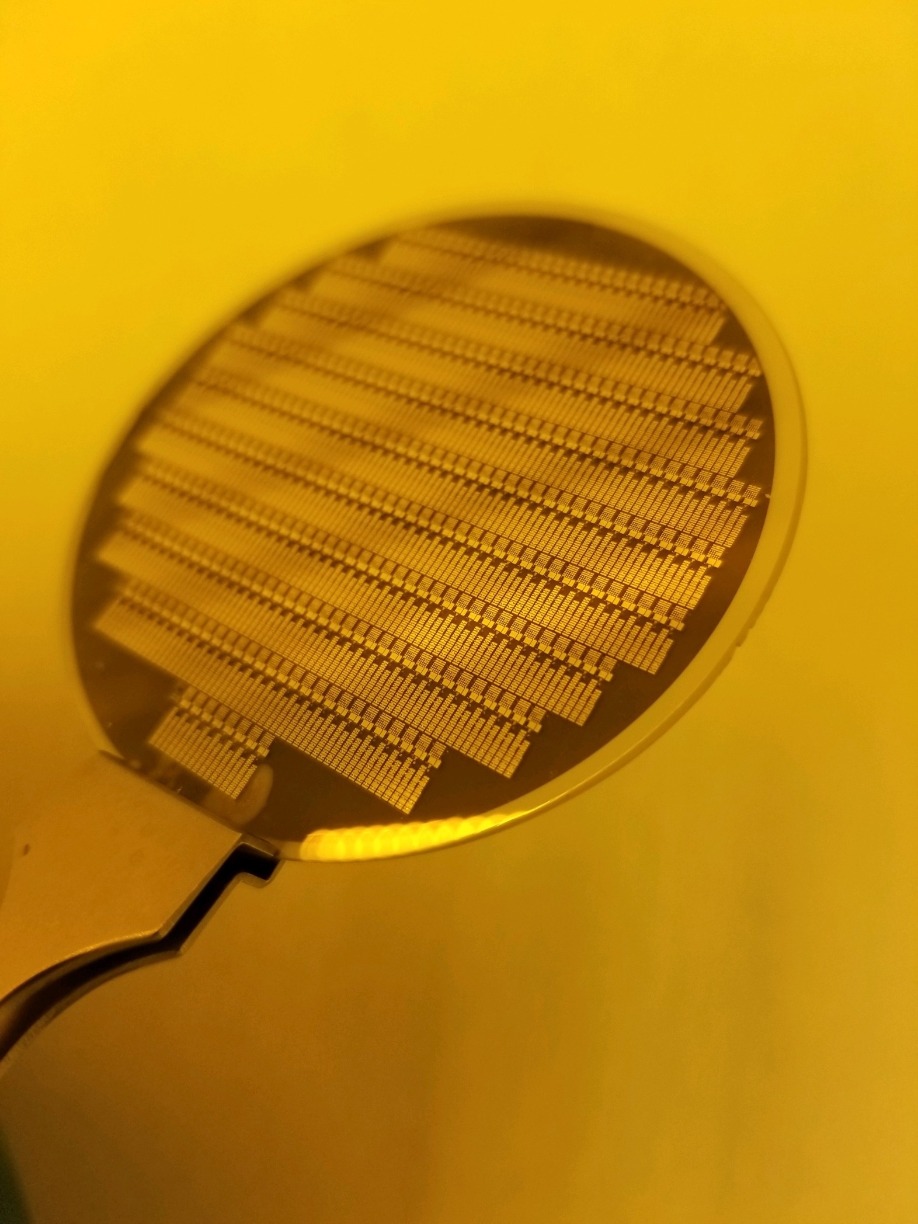
2-inch Synoptics gallium oxide substrate with an gallium oxide epitaxial layer and transistor fabrication completed by AFRL engineers.
Chabak drew inspiration not only from device results obtained with NICT’s MOSFET, but also: the availability of substrates, which can be produced from the melt; the opportunity for homoepitaxial growth with the β-phase of the material, leading to epitaxial films with a low defect density; and the simplicity associated with device fabrication. When the team fabricated their first device samples in 2015, Chabak wondered whether he and his co-workers could replicate the success of NICT and measure the purported high critical field strength.Despite his curiosity, Chabak did not intend to change direction and switch from working on GaN to gallium oxide: “We weren’t too invested in [gallium oxide] at the time. In fact, we were ready to pass on it if our early assessment of devices were to fail.”
To evaluate the potential of this ultra-wide bandgap material, Chabak and his colleagues leaned on their international partners for epistructures. Although they had access to MBE tools at AFRL, they were primarily configured for fundamental research in GaN (Chabak and colleagues have tremendous expertise in this area, following two decades of work providing rapid feedback to the GaN material community).
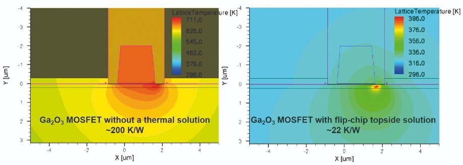
Technology computer-aided design simulation of thermal effects without and with a top-side solution implementing flip-chip technology, thickmetal contacts, a thermally conductive passivation dielectric on the channel and aggressive lateral scaling in a gallium oxide device.
Choosing to source gallium oxide epistructures initially actually had its benefits. It avoided having to procure expensive equipment and quickly gain epitaxial expertise in a new material. The team were also able to form valuable international materials partnerships to quickly move ahead on gallium oxide device research.Sourcing material
Substrates came from Tamura, the only commercial supplier. This firm, which has worked closely with NICT, uses the edge-defined, film-fed growth process to produce material that is up to 4-inch in diameter in some orientations. Substrate dimensions for one of the most common orientations were initially 10 mm by 15 mm, but in the last year Tamura has also started to offer variants that are 25 mm by 25 mm. There is no observed degradation in quality with the larger sizes, according to Chabak, while price per unit area has fallen by around 50 percent.
The team at AFRL purchased these substrates and contacted Tamura’s spin-off, Novel Crystal, to purchase epiwafers. In addition, the AFRL relied on another source of epitaxial growth, the Leibniz Institute for Crystal Growth, a facility more commonly known by the initials IKZ.
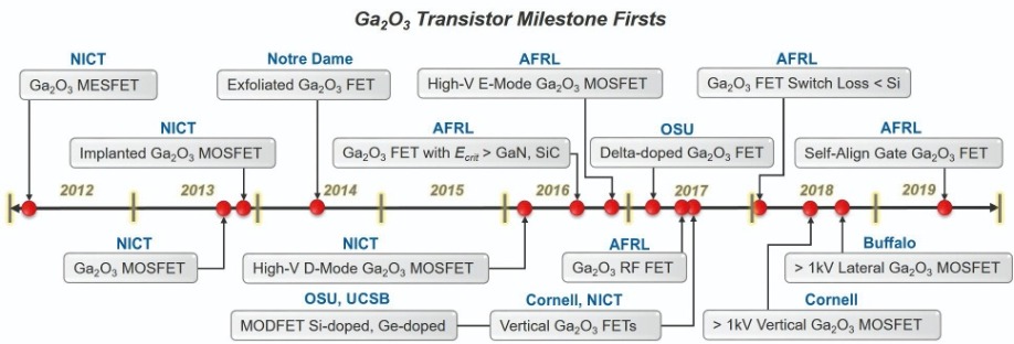
The researchers at AFRL have provided several significant contributions to the advance of gallium oxide devices.
In 2015, IKZ provided the first samples to the US team. Success followed, helping this German institute to become a valued research partner with AFRL. It is a relationship that has blossomed, with both sides actively engaging in collaborative research.By shipping high-quality material in good time, IKZ played a critical role in AFRL’s success. “We were able to become leaders in our field because we secured early access to materials,” admits Chabak.
The first milestone for this collaboration came in 2016, when AFRL device team member Andy Green fabricated and reported a MOSFET made from an IKZ epiwafer that blocked 230 V over a 0.6 μm gate-drain drift region. That translates to a record-breaking average critical field strength of 3.8 MV/cm. To put this figure in perspective, most lateral GaN devices, after a few decades of research, operate at 1 MV/cm. “So without much optimisation, we got about four times the critical field strength of GaN,” enthuses Chabak. “That was the spark that started the fire.”
Green’s record-breaking result came from an epiwafer made by MOCVD at IKZ, with growth on an off-cut substrate to optimise the diffusion length of the adatoms. Note, however, that Chabak and his colleagues have also obtained good results on MBE-grown material, provided by Novel Crystal, so they are yet to decide on what growth technique is better for gallium oxide homoepitaxy. “The jury is still out, we’ve made good devices on both, and we are still assessing materials.”
Side-stepping p-type problems
Later that year, the team from AFRL reported the first ever enhancement-mode FET with a high-voltage operation in the off-state. This ground-breaking result is important, as it shows that it is possible to fabricate a normally-off FET, despite the lack of p-type carriers in gallium oxide. Normally-off operation is highly valued, as it creates a device that is fail-safe, and can be driven with a unipolar power supply.
The key to this success is to employ the work function of the gate to pinch-off an array of non-planar fin channels. “We were the first ones to implement this with gallium oxide, but very similar things have been done with GaN,” says Chabak.
Note that it would have been folly for Chabak and his co-workers to try and attack problems associated with p-type doping in gallium oxide head on. Holes are self-trapped, so they fail to contribute to carrier transport, and the flatness in the valence band results in a very heavy hole mass.
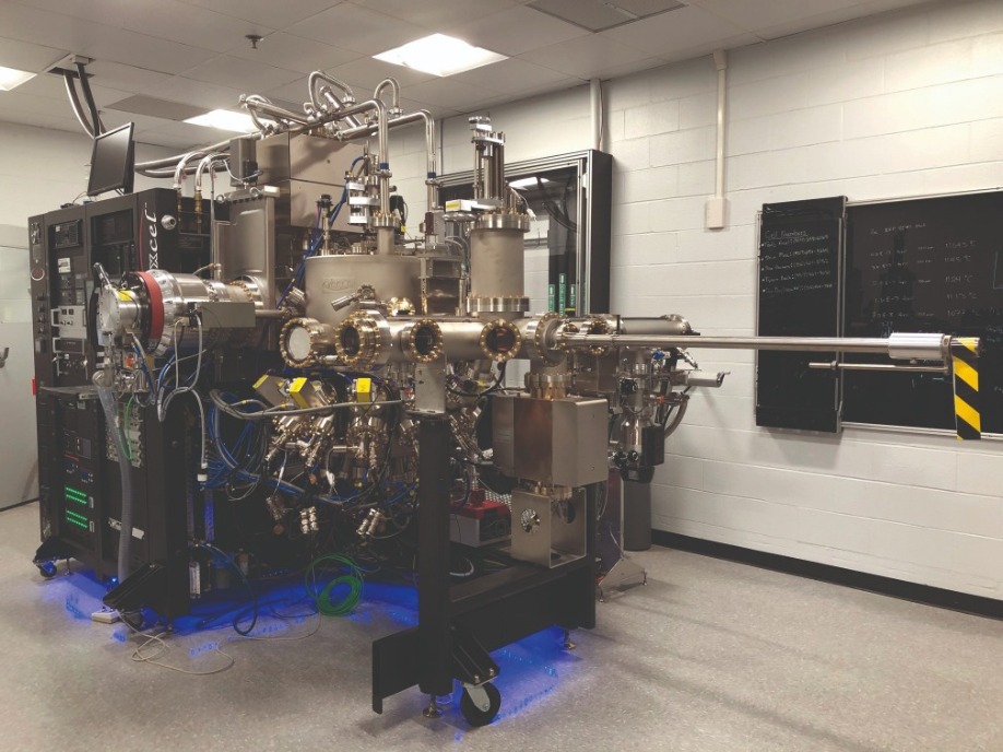
Veeco GenXcel oxide MBE tool located at AFRL dedicated to fundamental oxide materials and device research on up to 4-inch substrate sizes.
While p-doping is incredibly challenging, creating an abundance on unbound electrons in gallium oxide is relatively easy. There are three common dopants: silicon, tin and germanium. “All three of these dopants work, and we have made devices with them,” says Chabak. According to him, merits of silicon include its familiarity – it is widely used to dope GaN and GaAs – and the ease with which it can be introduced successfully within a growth chamber. To realise high concentrations, delta-doping and contact re-growth is possible, which produces good results.Implantation is another option for producing n-type material. Chabak views this as a tool that offers device engineering and lateral doping profiles, and allows the fabrication of transistors with self-aligned contacts – features that are difficult to implement in GaN.
Compared to wide bandgap materials, the temperature required to activate carriers in gallium oxide is quite low – in some circumstances, just 850 °C will suffice. Studies of this doping technique have led to some interesting results, such as finding that impurities diffuse along implanted, damaged regions.
Better than silicon
Chabak’s team claimed their third record-breaking result in 2018, when they reported the first gallium oxide FET with a switching loss below that for silicon. “There were a few different design tricks that were implemented,” reveals Chabak. Modifications included partially removing the channel to make it normally off, adding a gate-connected field plate to reduce the peak electric field and optimising device dimensions. Resistance fell by reducing the source-to-drain distance, a feat realised without sacrificing the breakdown voltage.
Efforts at AFRL have also included an investigation of the RF characteristics of gallium oxide transistors. “We are very careful to say that we do not see gallium oxide replacing gallium nitride for RF devices,” warns Chabak. “Gallium nitride devices will always be the king of RF power.” However, he thinks that gallium oxide could become a complementary technology, as transistors made from this material may have the potential to provide a high efficiency, or deliver a higher output power, when configured in a particular class of operation.
The team has investigated the RF characteristics of devices with a 0.7 μm gate length and a gate-recess, which reduces the channel thickness from 180 nm to around half that value. Small-signal measurements, using a drain-source voltage of 40 V, revealed a cut-off frequency and maximum oscillation frequency of 3 GHz and 13 GHz, respectively. Driven in class A mode, output power is 0.23 W mm-1 and the power added efficiency is 6.3 percent, according to CW large-signal power measurements at 800 MHz.
Severe heating limited the performance of these RF devices. That’s also the case for most power devices made from gallium oxide, as both types of device are impaired by the low thermal conductivity of this material. Some critics claim that this is a severe impediment for the progress of this class of device, but Chabak disagrees, arguing that it is not a “showstopper”. When discussing this issue with the naysayers, he is quick to point out that the thermal conductivity of GaAs, which is a mainstream RF power technology, is within an order of magnitude of that of gallium oxide.
To ensure that gallium oxide devices fulfil their potential, efforts will have to be directed at extracting heat from both the backside of the device, and the top, where the biggest gains can be made. “We have some preliminary modelling that suggests flip-chip technology can, when combined with backside wafer-thinning, reduce the overall thermal resistance of our devices to close to SiC.”
Realising such success will not be easy, admits Chabak. “I don't expect it to be something that is solved in the near term.” In fact, if significant progress is to be made, it will probably require the funding of major programmes. However, the approaches to explore this can draw on previous successes in the compound semiconductor industry. “Luckily we already have a lot of thermal management solutions, developed for gallium nitride and gallium arsenide. So we hope to take advantage of these.”
Chabak and his co-workers are not planning to tackle this problem just yet. Instead, they will direct their short-term efforts at introducing electron-beam lithography to the fabrication process, and scaling transistors to below a micron. The devices that result could be very attractive candidates for fast-switching applications, by combining very high speeds with high breakdown voltages.
The team mainly collaborates with their gallium oxide materials partners for epiwafers. But that should soon change, as last year the group invested in a state-of-the-art oxide MBE tool that can handle 4-inch substrates and produce gallium oxide epiwafers featuring either silicon or germanium doping. This reactor will also be used to produce heterostructures such as those containing aluminium gallium oxide.
Home-grown support
The introduction of the tool has expanded the number of researchers at the AFRL that are devoting at least some of their time to gallium oxide. A few years ago, efforts involved a smaller group of device engineers, all in the sensors group – but with the MBE machine on site and an exponential boom in interest, they now have participants from materials, devices and power groups across AFRL. “When we have meetings for gallium oxide, we can easily fill a large room now,” says Chabak.
Once epiwafer production is in-house, the team will only need to source substrates. In the near-term they will continue to come from Tamura, but further ahead, they could be obtained from a domestic source. That’s because AFRL has been funding a gallium oxide crystal growth programme at Synoptics, a subsidiary of Northrop Grumman.
“They are well ahead of the curve, because they have made crystals for lasers for a long time,” says Chabak. Using the Czochralski technique, Synoptics has been able to grow, fabricate and polish semi-insulating (010) substrates up to 2-inches in diameter.
In the last few months, the team at AFRL have started to make devices using these substrates. “Are they comparable to Tamura? Some are – we’re getting there,” says Chabak.
In addition to this funding, AFRL recently initiated a program with Saint Gobain for edge-fed film growth of semi-insulating, (010) 2-inch gallium oxide substrates.
Creating domestic sources for large area gallium oxide substrates will be the missing piece for Chabak and his device team. In turn, this should lead to enhanced research and development, giving the team from the AFRL a good chance to add to their tally of record-breaking results for gallium oxide devices.


