Slashing substrate costs for CPV
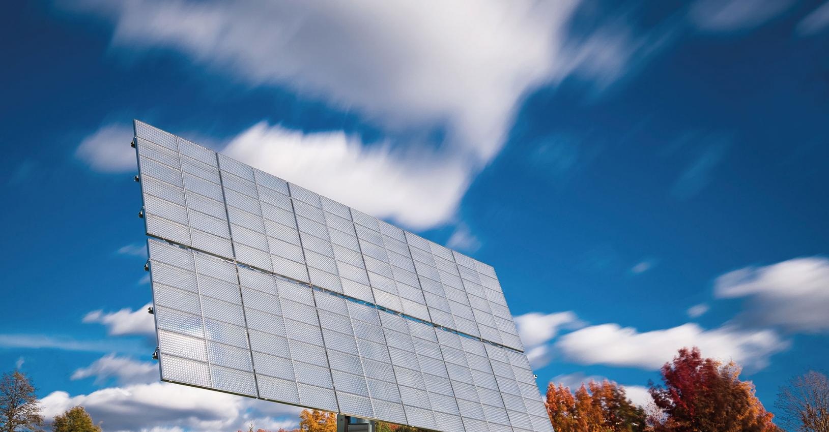
Switching to a silicon foundation and re-using germanium substrates offer two options for driving down the cost of multi-junction cells
BY RICHARD STEVENSON
THROUGH NO FAULT of its own, CPV may appear to have missed the boat. Many leading firms developing this technology have been killed off by a double whammy – a credit crunch that chocked further investment, and plummeting prices for silicon PV that blunted the competitive edge of this class of photovoltaics.
Given this state of affairs, it’s hard to see how CPV will ever make an impact. Today silicon dominates, and it is sure to do so for many years. But look further down the road and a more promising picture emerges. Any further gains in silicon cell efficiency are going to be marginal, limiting the performance of this technology, and production is already streamlined, so manufacturing costs are only going to show modest declines. This implies that electrical generation costs associated with silicon are only going to fall fractionally in the coming decades. Due to this, there is a good chance that CPV can catch up. And given its far higher efficiency than all forms of silicon single-junction cell, it promises to be particularly competitive in situations where the cost of land is at a premium, and there is a strong desire to generate as much power as possible from a plot.
To get CPV to a position where it has a chance of market success, efforts must be directed at investigating all the possibilities for increasing its competitiveness. Making cells more efficient, possibly through the use of more junctions, will improve the solar yield. Another lever is to reduce the cost of the tracker, along with making it lighter, as this trims shipping costs. And increasing the level of concentration is another promising option, as it allows fewer cells to generate a given output power.
Within this mix, there is also the opportunity to reduce the cost of the substrate. About one-tenth of the cost of the entire system is tied up in the cell, with the lion’s share attributed to its foundation. According to a study by the US National Renewable Energy Laboratory (NREL), in a GaAs solar cell the substrate accounts for 84 percent of the cost the device.
One group developing ways to cut the cost of the substrate is that led by Abderraouf Boucherif from the University of Sherbrooke in Quebec, Canada. His team, whose work is attracting much interest from industry, has not just developed one approach to slashing substrate costs – it has pioneered three distinct technologies. They are: introducing porosity to a germanium-on-silicon template, so that it can become a platform for making high-quality triple-junction cells; etching an epitaxial structure from its germanium substrate so that the latter can be re-used; and combining graphene and porous silicon to create a flexible, light-weight foundation for high-efficiency photovoltaics.
Porous silicon
The benefits of using a silicon substrate are not limited to a reduction in cost, but extend to a higher thermal conductivity, leading to a reduction in thermal management. According to Boucherif, in turn this diminishes the chance that a cell will ‘burn’, and increases its efficiency, thanks to a lower operating temperature. “These are not necessarily huge impacts, but it could give a little boost to the cell.”
Silicon is also stronger than germanium. This increases the robustness of the cell, and reduces the likelihood that a wafer will break during the fabrication process.
A third advantage of silicon over germanium is the larger diameter of the substrates, enabling an increase in manufacturing efficiency. This could be realised by processing in silicon fabs. A study by a team at the University of Ottawa has found that costs could reduce by up to 70 percent by switching the substrate from 100 mm germanium to 200 mm silicon.
The big concern with using silicon as the substrate for making triple-junction cells is the dislocation density in the epilayers. Dislocations degrade device performance by trapping the photogenerated carriers, dragging down efficiency.

Figure 1. When a germanium film is grown on silicon, the difference in lattice constants leads to the generation of many dislocations. These imperfections can be addressed with a process that begins with electrochemical porosification, which creates voids in the material. Annealing follows, with elevated temperatures promoting the coming together of two dislocations with opposite Burgess vectors that are attracted to the void. They glide together before annihilating, at which point they disappear from the surface and are trapped by the void. Dislocation-free material results, proving a platform for the growth of III-V cells.
When engineers deposit layers of III-Vs on silicon, the resulting dislocation density is typically 1 x 108 cm-2. “This is very high, and would reduce the efficiency of the cell dramatically,” explains Boucherif. He says that in order to ensure a high cell efficiency, the dislocation density must be no more than 5 x 106 cm-2.His team are able to produce germanium films on silicon substrates with a dislocation density well below this limit by using an electrochemical porosification process. According to Boucherif, this is a very simple, industry friendly self-organised process with very low costs. “No lithography or preparation steps are needed.”
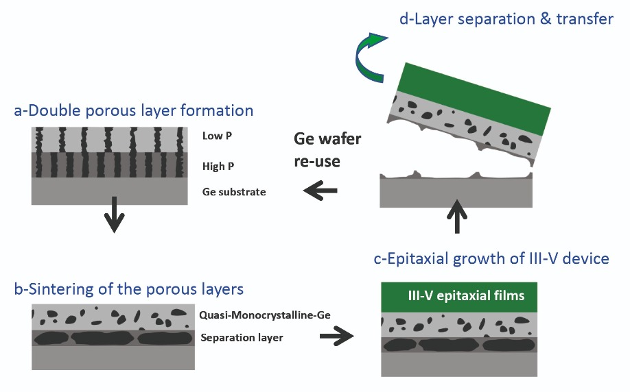
Figure 2. Re-use of germanium substrates begins with a formation of a high-porous and a low-porous layer (a). Sintering results in a quasi-crystalline germanium layer near the surface (b) that provides a platform for III-V growth (c). Electrochemical etching removes the separation layer and allows the substrate to be removed and reused.
Electrochemical porosification has been widely used in the silicon industry for many years. Silicon wafers are loaded in an electrochemical bath, and when a bias is applied nanopores form spontaneously. By varying the external current and adjusting the electrolyte, the size of these voids can be tuned from 5 nm to 100 nm.Boucherif and his co-workers have broken new ground by applying the process to germanium, rather than silicon. After growing a film of germanium-on-silicon, an electrochemical porosification process produces nano-scale voids in the epilayer (see Figure 1). Annealing at elevated temperatures for several minutes changes the profile of the pores in a process that irradiates dislocations, to yield a high-quality surface for subsequent III-V growth.
To demonstrate the power of this technique, the team have applied it to part of a 100 mm wafer, and compared the dislocation density to that of an untreated region. Using the electrochemical porosification process, the dislocation density plummets from around 107 cm-2 to just 104 cm-2.
Processed material is evaluated by scanning electron microscopy, transmission electron microscopy and X-ray diffraction. These techniques reveal that the team’s technology creates material that forms a barrier to dislocation propagation.
Germanium re-use
An alternative option for cutting cell costs is to continue to use germanium substrates for the growth of III-V cells, but after this, separate the active region from the substrate, which can be re-used.
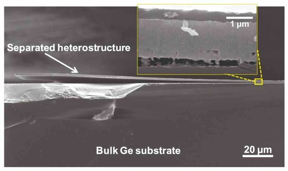
Figure 3. Separating the heterostructure from bulk material enables the re-use of germanium substrates.
“Germanium is more complex to etch,” explains Boucherif. “The silicon process doesn’t work if you apply it to germanium.” So the team at Sherbrooke have developed a bipolar etching process.Their approach begins by forming two regions within the germanium substrate: and upper layer, with a low porous density; on top of another layer with a higher porous density. Annealing transforms this into an upper quasi-monocrystalline layer sitting above a separation layer (see Figures 2). This step can be carried out by loading the material into an epi-reactor, and carrying out annealing prior to the growth of the III-V film. Separation follows, based on etching with a mixture of hydrofluoric acid and ethanol. For this, the team uses a two-step process, so that passivation can be applied after etching to prevent the dissolution of the removed germanium (see Figure 3).
Success with this approach has been proven by Boucherif and co-workers. They have grown a 400 nm-thick GaAs film on quasi-monocrystalline germanium. The GaAs is monocrystalline, according to X-ray diffraction.
Mesoporous silicon
The third solution proposed by the team is based on the use of mesoporous silicon, which is an incredibly flexible free-standing membrane. Its production involves porosification, followed by electro-polishing that creates free-standing material.
Unfortunately, mesoporous silicon is unsuitable for epitaxy, because it is unstable at the required growth temperatures. But Boucherif’s team has found that adding graphene addresses this weakness and allows epitaxy.
That is not the only change, however – it also introduces some strain. “That is one of the ways of adjusting the lattice parameters,” says Boucherif, who adds that the composite can also be used as a compliant substrate, because it is flexible and stable during epitaxial growth.
Very recently the team have used these mesoporous silicon and graphene structures as the foundation for the growth of GaN films. That might seem an odd choice, since GaN is not used in multi-junction cells. However, there is a good reason for growing this material – as it requires a very high growth temperature, if success results, it should be possible to apply this technology to all III-V film growth.
Comparing the quality of this GaN to that grown on bulk silicon reveals an improvement. “We see a reduction in crack density,” says Boucherif, who is quick to point out that more work must be done before high-quality GaN epilayers are produced.
From materials to devices
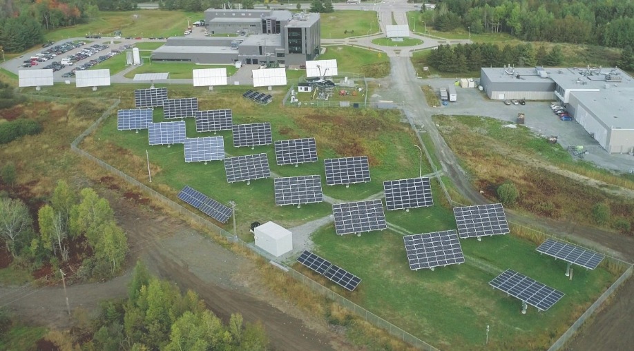
Additional plans for the future include a shift from characterising materials to evaluating devices. For that objective, Boucherif and his team could not be better placed – the university has a solar park on its campus that has been up and running for a year, and provides a test site for various photovoltaic and thermal solar technologies.
As well as generating up to 1 MW of power – that equates to about 15 percent of the university’s electricity needs – the site is helping to evaluate the reliability and performance of solar cell technologies under a variety of weather conditions. “In Quebec, we have in summer more than 30 degrees, and in winter down to minus 25,” says Boucherif.
Devices made by his team can be placed in one of eight CPV systems, each with a peak output of 30 kW, based on a technology that originated at Concentrix. All the systems have been deployed by Saint-Augustin Canada Electric Inc (STACE), which manufactures the CPV systems in Trois-rivieres in Quebec, Canada, using carbon-free hydro-electricity.
The solar park is clearly going to play a role on the future development of terrestrial triple-junction technology. This facility will hopefully demonstrate that it is possible to make reliable, highly efficient multi-junction cells that are free from high substrate costs, and ultimately help to rekindle the prospects for CPV technology.
Y. Bioud et al. Nat. Commun. 10 4322 (2019)
A. Boucherif et al. Appl. Phys. Lett. 102 011915 (2013)
J. Ward et al. Prog. Photovolt: Res. Appl. 24 1284 (2016)


