


Getting ready for GaN CMOS

Aggressively scaled p-channel GaN transistors, formed on the same epiwafers as their n-type cousins, offer a very promising route to power electronic circuits made with a CMOS technology
BY NADIM CHOWDHURY AND TOMÁS PALACOIS FROM MIT
THE POWER ELECTRONIC CIRCUIT looks set to play an ever-increasing role in all our lives. It is needed in data centres, electric vehicles, cloud computing, and the internet of things.
Often, the performance of this type of circuit is far from ideal. Efficiency is below where it could be, and the circuit takes up much space, due to the use of bulky passive components, such as large inductors and capacitors. What’s needed is to move to more efficient transistors that switch at faster speed. Do this and many benefits result – as well as trimming the electrical losses associated with this device, a higher switching frequency allows the use of smaller passive components that shrink the size and weight of the circuit.
One option for ushering in the era of better circuits is to replace silicon transistors with those made from GaN. Moving to this wide band gap material leads to an increase in the critical electric field strength, making it suitable for high-voltage applications. In addition GaN is renowned for its high saturation velocity, aiding high-frequency operation; and its low on-resistance, enabling low switching losses.
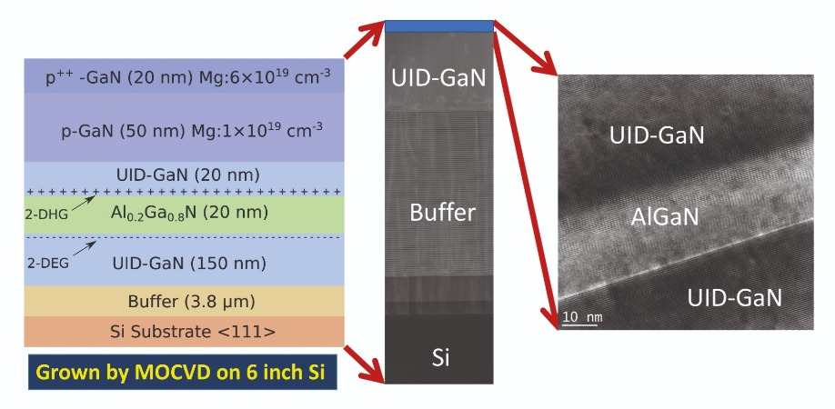
Figure 1. The designed epilayer for p-FETs, along with a transmission electron microscopy image. The structure is as follows: 20 nm p++-GaN (Mg: 6×1019 cm-3 with 2–3 percent activation at room temperature), 50 nm p-GaN (Mg: 1019 cm-3), 20 nm unintentionally doped GaN (Si: 5×1016 cm-3), 20 nm Al0.2Ga0.8N (Si: 5×1016 cm-3), 150 nm unintentionally doped GaN (Si: 5×1016 cm-3), 3.8 μm buffer and silicon substrate.
Unfortunately, the potential of GaN is yet to be unleashed. In most commercial applications where GaN power transistors are deployed, they are not switching at gigahertz or megahertz frequencies. Instead they are plodding along in the kilohertz domain, primarily to accommodate voltage instabilities caused by the inductance between the gate of the power transistor and the off-chip gate driver circuits. To break the shackles, there must be an introduction of a GaN CMOS technology. This will open the door to integrated GaN gate driver circuits that are more efficient, and have a reduced form factor that leads to an increased power density. Merits of such a technology are the consumption of almost zero static power, higher linearity and the opportunity for rail-to-rail voltage swings.A major road block towards realising such a technology is the sub-par performance of the GaN p-FET. Compounding this issue, it’s also not easy to find a way to deliver on-chip integration of this device with its partner, an E-mode n-FET. But at MIT we have succeeded on both fronts. Efforts in our lab have culminated in an E-mode p-FET that is easy to integrate with an E-mode, n-type counterpart. The E-mode p-FET delivers great performance, sporting a record low on-resistance, and it produces E-mode operation with a threshold voltage of -1 V .
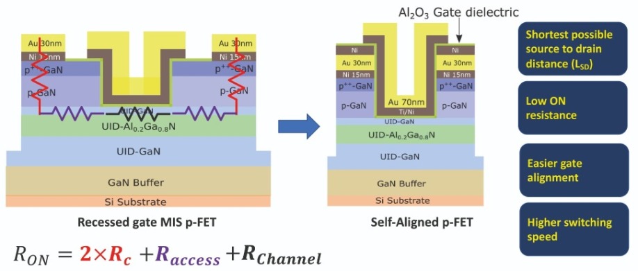
Figure 2. The self-aligned p-FET pioneered by MIT has several advantages over the recessed gate MIS p-FET.
To produce a high-performance GaN p-FET, we have overcome challenges associated with the low hole density in doped p-GaN, the difficulties in forming an ohmic contact, and the low hole mobility in this material. It is well known that magnesium, the most common p-type dopant in GaN, has a relatively high activation energy – typically, it is between 150 meV and 200 meV. Due to this, only 1 percent to 2 percent of the dopants are activated at room temperature, leading to a very low hole density. To overcome this, we have turned to a III-N heterostructure as the source of holes, employing it as the channel for the transistor. This has the added advantage of removing temperature dependence, as the two-dimensional hole gas channel provides carriers through a polarization difference, rather than the activation of dopants.A metal with a very high work function is needed to form a good ohmic contact for the holes in GaN. Nickel oxide is a good choice, due to its work function of around 6.3 eV. By using this oxide, we ensure a relatively good ohmic contact to the two-dimensional hole gas.
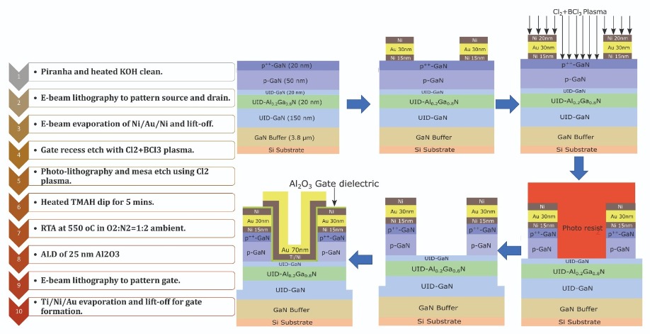
Figure 3. Key process steps for realising the self-aligned p-FET, along with illustrations for each step.
Increasing the hole mobility from 40-10 cm2 V-1 s-1 is far from easy, due to the high effective mass for holes in GaN. Rather than trying to tackle this daunting issue head-on, we simply aggressively scale the device to reduce the transit time of holes from source to drain.
Fabricating pFETs…
To avoid any complications that come from regrowth technology, we use an epilayer design that facilitates both n-FETs and p-FETs. We have undertaken extensive device simulations with TCAD to determine the exact dimensions and the compositions of the layers in this heterostructure (see Figure 1), which we have produced by MOCVD on a 6-inch, 1 mm-thick silicon (111) substrate.
One of the features of this design is the provision of a source of p-type carriers from the polarization-induced two-dimensional hole gas at the interface of the top unintentionally-doped GaN/AlGaN heterostructure. To enabled good ohmic contact to this hole gas, we use a heavily p-doped top GaN layer; and to increase hole mobility, we include a 20 nm-thick unintentionally-doped GaN layer to separate the p-GaN and AlGaN layers. Hall measurements suggest these schemes are successful, as the two-dimensional hole gas density and the drift mobility are 8×1012 cm-2 and 11 cm2 V-1 s-1.
We are not alone in developing a p-type GaN FET. However, while most groups have pursued recessed gate MISFET structures (see Figure 2), we have directed our efforts at a self-aligned architecture. In our view, it has the upper hand on three fronts: it has the shortest possible source to drain distance, cutting down the access region; it has a low on-resistance, thanks to a negligible access resistance; and it simplifies gate alignment.
To produce FETs from our epiwafers, we begin by using electron beam lithography to create source and drain electrodes. Electron-beam evaporation adds a metal stack – 20 nm of nickel, followed by 30 nm of gold and another 20 nm of nickel – prior to a lift-off step using acetone. After this, we use an inductively coupled plasma, reactive-ion etch (ICP-RIE) to provide a blank etch, a step that helps with the formation of the gate recess. During this etch, the top 20 nm-thick film of nickel on the source and drain metal serves as a mask, protecting the ohmic contact from damage. The etch depth is controlled by the etch time. Following this, the mesa etch is performed by an ICP-RIE process, using a photoresist mask and a combination of chlorine and boron trichloride gases.
After all these etching steps, we remove the photoresist and reduce the etch-induced roughness by dipping the sample into heated tetramethylammonium hydroxide for about 15 minutes. We then add about 30 nm of Al2O3 by atomic layer deposition, to create a gate dielectric. Finally, using electron-beam evaporation and lift-off, we form a gate metal electrode, comprising 10 nm-thick titanium, 20 nm-thick nickel and 100 nm-thick gold (note that our entire process is summarised in Figure 3). We have imaged a cross-section of this fabricated device with a scanning transmission electron microscope (see Figure 4).
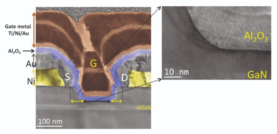
Figure 4. Transmission electron microscopy (TEM) image of the fabricated self-aligned p-FET with a 100 nm channel length. A zoomed TEM image shows the smooth interface between the GaN and gate dielectric, attesting to the high quality of the gate recess process with low surface roughness.
… and evaluating themOur p-FETs have an on-off ratio of 6×10⁵ and gate leakage that is typically just 1 nA/mm (see Figure 5(a)). In the off-state, the drain leakage current of these transistors is limited by gate leakage. This leakage is high in the off-state, due to high electric fields between gate and drain terminals, and across the gate dielectric at the sidewall of the gate recess.
The E-mode operation of our FET is seen in the plots of the drain-source current as a function of gate-source voltage (see Figure 5(b)). These measurements reveal a threshold voltage of -1 V. When transconductance is graphed as a function of gate-source voltage, maximum transconductance is shown to be 0.9 mS/mm at -4 V, for a drain-source voltage of -1.5 V. Measuring the output characteristics reveals good pinch-off and an on-resistance of about 400 Ω mm.
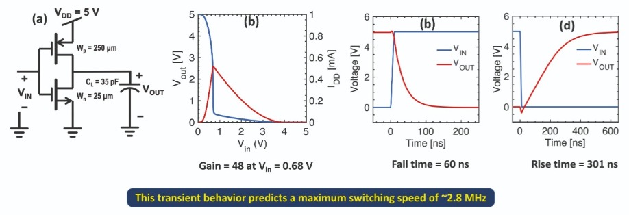
Figure 5. (a) Semi-log plot of IDS vs VGS at VDS=−0.5 V, demonstrating an on-off ratio of 6×10⁵. In the on-state, the gate leakage current is only in the range of 1 nA/mm. However, an increase in gate leakage is observed in the off-state, mainly due to the high electric field at the drain-end of the transistor. (b) Linear scale plot of IDS vs VGS, demonstrating a threshold voltage of −1 V. (c) Measured gm vs VGS characteristics with a peak transconductance of 0.9 mS/mm. (d) Measured IDS vs VDS characteristics, demonstrating an on-resistance of 400 Ω·mm at VGS=−7 V (this is calculated by taking an inverse slope in the low VDS regime of the output characteristics). The plot also shows an on-current density of more than 5 mA/mm at VGS=−7 V and VDS=−5 V.
We have benchmarked the performance of our self-aligned p-FET against other p-channel transistors reported in the literature, using the on-resistance and the on-off ratio as key GaN metrics (see Figure 6). This exercise highlights the superiority of our transistors. Note that the GaN/AlInGaN based p-FETs produced by other groups have a slightly lower resistance than our self-aligned p-FETs. This is due to the high two-dimensional hole gas density produced by a large negative polarization charge at the III-N hetero-interface that leads to undesirable, normally on operation.When comparing various results, it should be remembered that our p-FET has the additional advantage of having a two-dimensional electron gas beneath the two-dimensional hole gas − this holds the key to making an on-chip n-channel transistor with the same epi-structure, without having to resort to any regrowth. When evaluating these transistors, it also important to bear in mind that our p-FET shows E-mode operation, unlike many devices reported in the literature so far.
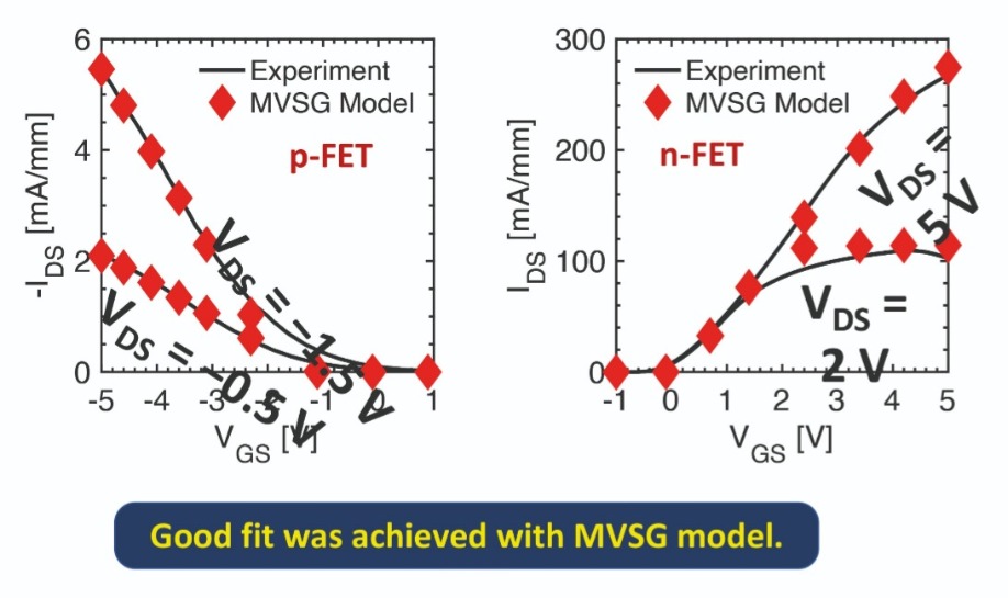
Figure 6. Benchmarking of the reported self-aligned p-FET with other demonstrated p-FETs in the literature in terms of on-resistance and on-off ratio. It is quite evident that the reported device is closest to the desired region exhibiting an on-resistance of 400 Ω mm with excellent on-off ratio of 6×10⁵. The p-FET produced by MIT enables easy integration with an on-chip n-FET without any regrowth, as illustrated in Figure 7(a). The device is E-mode with −1 V threshold voltage. MIT’s FET shows record on-resistance and on-off ratio for any GaN-based E-mode p-FET, making it a promising candidate for GaN-based complementary logic.
We have also produced an n-channel GaN FET with our epiwafers (see Figure 7(a)). The threshold voltage from this monolithically integrated n-FET is 0.2 V. To increase the value of this p-GaN gated n-FET while retaining the epistructure, we could turn to a FinFET or nanoribbon structure. The output characteristics of our n-channel FET include an on-resistance of 19 Ω mm and an on-current that exceeds 200 mA/mm (see Figure 7(c)).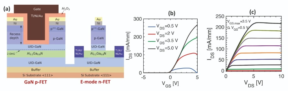
Figure 7. (a) Monolithic integration of a self-aligned p-FET and p-GaN gated n-FET. (b) IDS vs VGS characteristics of the n-FET, using in linear scale. This reveals a threshold voltage of 0.2 V. (c) IDS vs VDS characteristics of the n-channel FET.
To evaluate the potential of the monolithic integration of our p-FET and n-FET for GaN-based CMOS applications, we have turned to circuit simulations. They have been undertaken with the Cadence Virtuoso tool, with compact models for the devices obtained using the industry-standard MIT Virtual Source GaN-FET compact model (see Figure 8).
Figure 8. Compact modelling of both a p-FET and an n-FET using an MIT Virtual Source GaN-FET model yields a good fit with experimental results.
Results of these calculations are encouraging (see Figure 9 for details of the inverter circuit and simulation methodology). Simulations of voltage transfer curves, for a 5V DC bias and n-FET and p-FET gate widths of 25 μm and 250 μm, determine a maximum voltage gain of 48 for an input voltage of 0.68 V. The DC current drawn by the inverter peaks at 0.52 mA when the input voltage is 0.70 V. This is the switching point of the inverter.We have studied the switching behaviour of the inverter by applying a capacitive load of 35 pF. The rise time is just 60 ns, far shorter than the fall time of 301 ns, which is compromised by the high on-resistance of the p-FET. However, this fall time is still short enough to yield a switching speed of 2.5 MHz, which is sufficient for most power electronic applications.
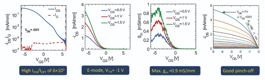
Figure 9. (a) Circuit diagram and methodology used in MIT’s simulation of the GaN-based complementary logic inverter. (b) Voltage transfer curve of the GaN-based complementary logic inverter. The n-FET and p-FET have gate widths of 25 μm and 250 μm, respectively. Simulated waveforms showing the (c) fall and (d) rise edge of the output signal from the inverter. The rise/fall time of the input signal is 10 ns. The fall and rise times of the output signal are 60 ns and 301 ns, respectively.
Our team is buoyed by this success, coming from the integration of 100 nm channel length GaN p-FETs, which are the first to be made on 150 mm silicon wafers, with GaN n-FETs. This is a significant step towards high-performance GaN CMOS technology. While there is still room for significant improvement, our demonstration opens up several application domains for GaN, including integrated CMOS driver circuits, CMOS logic, harsh environment computation and control electronics, and high-voltage analog and mixed-signal circuits.N. Chowdhury et al. “First Demonstration of Self-Aligned pFET on Si”, IEEE International Electron Device Meeting, 2019
N. Chowdhury et al. IEEE Electron Device Lett. 41 (2020) DOI:10.1109/LED.2020.2987003
N. Chowdhury et al. IEEE Electron Device Lett. 40 1036 (2019)
N. Chowdhury, “p-Channel gallium nitride transistor on Si substrate,” Masters diss., Massachusetts Institute of Technology, 2018