

Designing MMICs for millimetre-wave 5G

High-performance front-ends for millimetre-wave 5G require powerful and efficient GaAs ICs that are housed in carefully chosen packages
BY LIAM DEVLIN, ANDY DEARN, STUART GLYNN, GRAHAM PEARSON, ROBERT SMITH AND MOHAMMED TAHIR FROM PLEXTEK RFI
TO ADDRESS the growing demand for higher data rates and increased capacity, the latest generation of cellular communications is expanding its spectrum usage to include millimetre-wave frequency bands. This move has its pros and cons: it opens up significant opportunities for the compound semiconductors industry, but creates considerable challenges for designers of front-end ICs for 5G applications.
Our team at Plextek RFI (PRFI) is taking on these challenges as we play our part in the roll-out of millimetre-wave 5G. Our efforts include designing and realising a number of custom GaAs ICs, and measuring their performance. Here we detail this work and discuss the challenges of implementing packaging at millimetre-wave frequencies using low-cost surface-mount technology (SMT), and the techniques that can be adopted to ensure the high-performance packaged parts.
Working with GaAs
Millimetre-wave power amplifiers (PAs) based on GaAs technology provide a much higher power density than silicon technologies, as well as a superior power-added efficiency. Using a 0.15 μm gate length E-mode PHEMT process from WIN Semiconductors, we have designed a 28 GHz PA, which we assembled into a 20-pin 4 mm x 4 mm over-moulded plastic QFN (quad-flat, no-leads) package (see Figure 1). To assess its performance, we mounted this packaged PA on a representative evaluation PCB.
The PA in this package is a three-stage design. Its output stage comprises four identical transistors, configured with a power-combining matching network at the output. Such an approach is essential at millimetre-wave frequencies. While in theory, as a transistor is made larger – either by adding more gate fingers or increasing the unit gate width – there is a proportional rise in RF output power capability, in practice this simple approach cannot be adopted at higher frequencies. The problem is that as size increases additional parasitics kick-in at higher frequencies, compromising available gain. So a sweet spot must be found size-wise to balance the competing requirements for gain and RF output power.
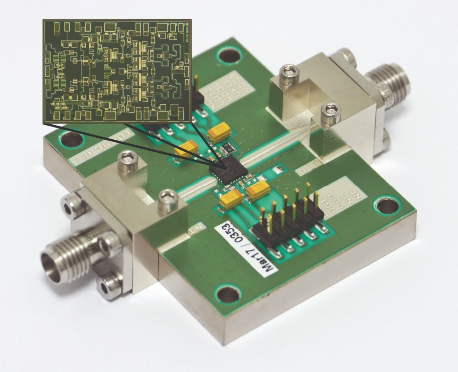
Figure 1. A surface mount technology (SMT) packaged 28 GHz 5G PA that has been developed by PRFI and mounted on an evaluation PCB. A power-combining output-matching network is visible to the right hand side of the die photograph.
We use output power sampling with temperature compensation to allow measureement of the transmitted RF power. We drive the four output transistors with a pair of driver devices, which are in turn are driven with a smaller pre-driver. One of the merits of selecting an E–mode process is that the gates are biased with a positive voltage, so there is no need for a negative supply voltage as required by most D-mode pHEMT PAs. We bias the entire PA from a +4 V drain supply.
A fast-switching enable circuit is also included on-chip. It can be used to rapidly power up and power down the PA. By drawing just 0.1 mA when not in use, it helps maximise overall system efficiency.
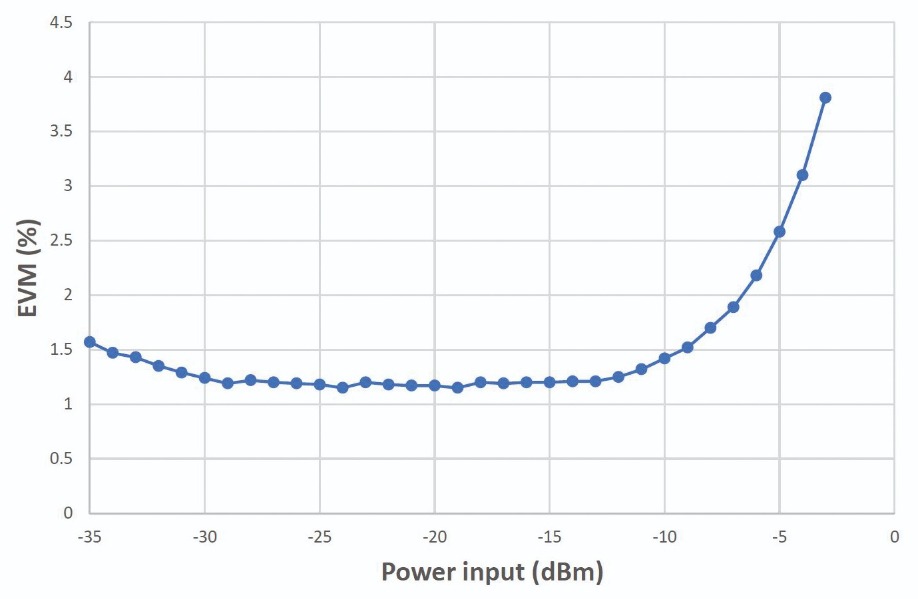
Figure 2. Error vector magnitude (EVM) of the packaged PRFI PA versus PA input power at 28 GHz, OFDM 400 MHz, 64 QAM. At an operating point of 18 dBm average output power, the input power is -3 dBm and the EVM is less than 4 percent.
Like the majority of PAs employed in a 5G communications system, we operate our design backed-off from compression, so that we can preserve the modulation fidelity of the transmitted signal. This is accomplished with a deep class AB bias scheme. Our design efforts begin by selecting the optimum transistor size for the output stage. After this, we simulate load-pull conditions to determine the optimum impedances for best linearity and power-added efficiency at back-off, considering different quiescent bias conditions. Evaluation of the gain, linearity and power-added efficiency follow, enabling us to determine the optimum bias condition. Measurements reveal good performance across the 28 GHz 5G band that spans from 27.5 GHz to 28.35 GHz, using biasing that ensures a 180 mA total quiescent current from +4 V. For this PA the small signal gain is above 20 dB, and the input return loss exceeds 16 dB across the entire band.
We have designed this PA for optimum third-order intermodulation performance and power-added efficiency when backed off by 7 dB below the +25 dBm output power 1 dB compression point; such conditions are close to those that we would expect to be used in a 5G system incorporating this amplifier. According to our measurements, power-added efficiency at P-1dB is around 25.5 percent, rising to 30 percent at the top of the band, and the efficiency of the packaged part at the operating point is 8 percent. While this may not appear to be an impressive result, it is competitive performance for a class AB amplifier operating at this level of back-off.
Another measurement that we have carried out is a two-tone intermodulation test at +18 dBm output. This revealed a level for a metric referred to as the third-order intercept point (OIP3) of +32.5 dBm for an IMD3 of -35 dBc.
The performance of our PA has also been evaluated using a real wideband 5G signal: a 400 MHz bandwidth OFDM signal that has sub carriers every 120 kHz running 64QAM, and a peak-to-average ratio of 11.7 dB. When the PA is transmitting this signal, it has a high degree of linearity, which is evident from a plot of the error vector magnitude against input power at 28 GHz (see Figure 2).
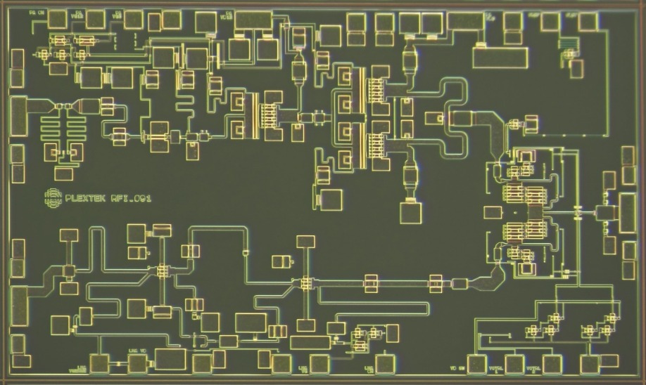
Figure 3. Die photograph of a PRFI 28 GHz front-end module (FEM). The PA runs from left to right along the top of the die photograph, and the Tx/Rx switch can be seen in the centre right of the die. The low-noise amplifier (LNA) runs from right to left, with RF output towards the bottom of the left-hand edge of the die.
Perfecting the package
In consumer electronics, surface mount technology (SMT) dominates the assembly process. Consequently, if millimetre-wave 5G components are to be commercially successful, they must be available in SMT-compatible packages. The most common, lowest-cost form of this for microwave and millimetre-wave components is over-moulded plastic, used for the 28 GHz PA that we have described (shown in Figure 1). For this amplifier, the style is QFN, which is the most popular SMT package for microwave ICs. It features a solid metal base, which is solder-attached to a ground plane on the PCB. Merits of this include a good thermal contact and a low inductance contact to PCB ground.
If an IC is designed for best performance as a die, with no consideration given to packaging, and this chip is assembled into a package – even one with a style already used effectively for millimetre-wave ICs – the performance is severely degraded. To ensure that the package does not hamper performance, there is a need to carefully consider the impact of: the moulding compound in direct contact with the surface of the IC; the inductance of bondwires, and the transition from the die through the package to the PCB; the physical size of the package leadframe, which has the potential to be resonant in-band; and the grounding inductance between the IC ground and the PCB ground.
During the design process, we use electromagnetic simulations to evaluate the impact of the moulding compound. Ultimately, it is the performance of the packaged IC on the PCB that is of most importance, so the design must be optimised for this. Many available IC processes include a passivation layer on the surface of the die that mitigates the effects of the plastic. Other options for housing the PA include air-cavity plastic packages and other forms of SMT that have an air cavity, such as laminate, ceramic or liquid crystal polymer. Although all are available as standard ‘open-tooled’ packages, custom designs can be used to optimise the performance of a particular IC.
We know that the inductance of the bondwire can severely degrade the performance of a millimetre-wave IC. Our first step to minimising the impact of this inductance is to trim the length of the bond interconnect, by co-designing the IC and package. Further reductions in inductance result from using multiple bondwires: our packaged millimetre-wave ICs tend to have two or three bonds to the RF pads. As well as taking these steps, we incorporate the series inductance of the bondwires into a low-pass filter that also comprises the capacitance of the RF pad on the IC, the series inductance of the package lead, and the capacitance of the package SMT pad to the PCB ground.
The 5 mm x 5 mm packages that we use have a corner-to-corner distance of just over 7 mm. This gives rise to a potential for resonance at 21.4 GHz – the frequency that corresponds to half a wavelength in air. The presence of moulding compound increases the effective electrical dimensions, leading to a lower resonant frequency. Due to this, there is a danger that the physical size of the package will result in an in-band resonance at millimetre-wave frequencies. To prevent this, we use an appropriate design for the custom leadframe, with selected pins directly connected to the die attach paddle. In addition, we give much thought to the design of the PCB on which the packaged IC is mounted.
For ICs made from GaAs and GaN, the backside of the chip is normally the RF ground. A low-inductance connection to this is made with the die attach paddle in the QFN style package. Using this approach, the exposed paddle on the back of the package is normally connected to the PCB ground.
When adopting this approach, it is vital to ensure a sufficiently low inductance for the IC to PCB ground connection. Much consideration must be given to the grounding inductance, as it is a source of series inductive feedback around the IC. If this inductance is too high it degrades performance – and in the worst case, it even causes instability. This can be avoided by using thin substrate material and multiple connections from the paddle to PCB ground.
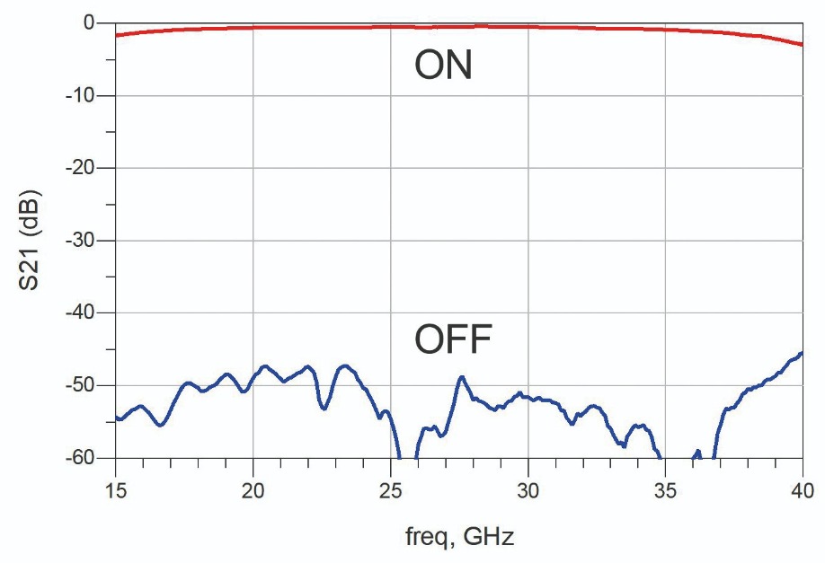
Figure 4. RF on-wafer measured on-state and off-state performance of a typical switch.
Packaging front-end modules
We have also used GaAs technology to design more highly integrated front-end millimetre-wave components. They include a front-end module for the 28 GHz 5G band comprising a three-stage PA, RF transmit power detector, Tx/Rx switch and two-stage low-noise amplifier (see Figure 3). Again, this IC has been designed using WIN’s 0.15 μm gate length E-mode pHEMT process that was used for the PA, and has been housed in a 5 mm by 5 mm over-moulded plastic QFN package.
One can view the PA in this front-end IC as essentially half of the PA MMIC described above. That is, rather than four transistors for the output stage, there are two. It thus has around half the RF output power capability of the MMIC with four transistors, but offers a similar level of gain. It also features a temperature-compensated RF output power detector.
In this module, the Tx/Rx switch connects the RF common port of the IC to either the PA output or the low-noise amplifier input. By arranging multiple switching transistors in a cascade configuration, power handling improves, and linear operation is ensured at the desired RF output level.
To bring the point of optimum noise match closer to the point of best return loss, we use series inductive feedback in the low-noise amplifier. A stacked bias scheme is adopted, with the same DC current running through both transistors to provide an Rx path gain of 13.5 dB with a supply current of just 10 mA from a +4 V source.
For the transmit path, output power is just over 20 dBm at 1 dB gain compression, with a power-added efficiency of 20 percent. These figures come from measurements on a packaged part that is assembled onto a representative evaluation PCB. Design has been optimised for high efficiency, when backed-off for linear operation with an IMD3 of -35 dBc. Using a 100 MHz tone spacing, OIP3 is around +28 dBm across the 5G band. There is very little variation with tone power over a 10 dB dynamic range.
Additional measurements reveal that the receive path gain is 13.5 dB and the noise figure 3.3 dB. This path has impressive linearity – OIP3 is 20 dBm, for a DC power consumption of just 40 mW.
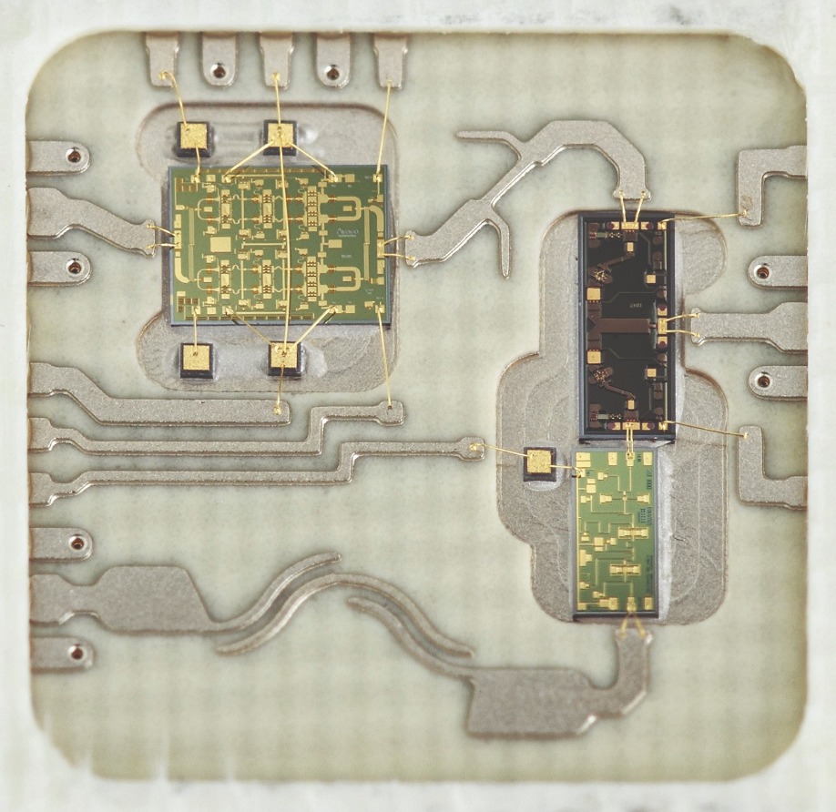
Figure 5. A 26 GHz 5G front-end, multichip module designed by PRFI and housed in a custom laminate package. The PA is the largest die, seen in the top left of the photograph. The Tx/Rx switch is to the centre right of the photo, the common RF Tx/Rx port is to the right of the switch die on the centre right edge with its ground-signal-ground through-package transition clearly visible. The Tx port of the switch connects to the harmonic filter at the top of the switch die and the Rx port at the bottom of the switch die connects directly to the low-noise amplifier input.
Low-loss MMIC switches
Most commercially available RF and microwave switches are based on FETs, produced using either pHEMT or SOI processes. Unfortunately, as the operating frequency increases, it becomes ever-more challenging to design this class of switch. The biggest issue is that although the drain-source resistance of the FET is high when pinched-off, there is a parallel parasitic capacitance that becomes significant at higher frequencies, offering a low-impedance path to RF signals. One option for trimming this capacitance is to turn to smaller transistors, but this produces a hike in on-state loss, and power handling is compromised.
Instead, we advocate the use of p-i-n diode switches for millimetre-wave applications. One of their best attributes is that, for a comparable on-state resistance, they provide a much lower parasitic off-state capacitance than FETs. This leads to a low insertion loss and high isolation at millimetre-wave frequencies. Another merit of the p-i-n diode is that it behaves as a current-controlled resistor at RF and microwave frequencies. As this class of diode can also be optimised to provide a wide resistance range, good linearity and high-power handling capability, it is an excellent choice for making RF and microwave switches.
Although the off-state capacitance of the p-i-n diode is very low, it can still represent a significantly low reactance at millimetre-wave frequencies. For example, if the off-state capacitance is just 0.05 pF, this would reduce the isolation of a series-mounted off-state device to just 3.6 dB at 28 GHz. To ensure high isolation, we use shunt mounted diodes to provide a low-resistance path to ground in the on-state. When series and shunt diodes are combined, the broadband switches that result can span from near DC to millimetre-wave frequencies. If operation down to such low frequencies is not required, then switches can be built using just shunt devices. A bandpass response results, but with the advantage of lower insertion loss at millimetre-wave frequencies, thanks to the absence of series devices.
We have designed SPDT, SP4T and DPDT millimetre-wave switch MMICs using p-i-n diode processes. Taking RF on-wafer measurements allows us to compare on-state loss with off-state isolation for a SPDT switch that has two shunt-mounted p-i-n diodes in each arm (see Figure 4). When the diodes are ‘on’ they provide a low resistance to ground and a high isolation through that branch; and when they are ‘off’ they have a small shunt capacitance, which is absorbed into a low-pass filter, resulting in a low insertion loss through that branch. Our RF on-wafer measurements reveal an on-state loss of just 0.55 dB ± 0.1 dB across the 20 GHz to 32 GHz range, with isolation exceeding 47 dB.
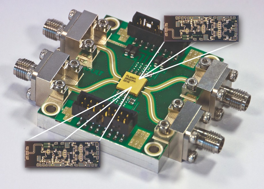
Figure 6. PRFI’s dual-channel 26 GHz PA in custom laminate package. The measured S22 of the packaged part improves at the top of the band compared to the bare die. S22 is less than -12.5 dB from 24 GHz to 28 GHz. The S11 degrades slightly compared to the bare die, but is still less than -10 dB.
Multi-chip modules
Another class of design is a millimetre-wave multi-chip module, made with surface-mount technology and formed using laminate packaging. Using this approach, we have created a multi-chip front-end module housed in a 10 mm x 10 mm laminate QFN package (see Figure 5). Manufacturing and assembly have been undertaken by Filtronic, UK.
The multi-chip module includes three commercially available die: a p-i-n diode SPDT Tx/Rx switch, a pHEMT low-noise amplifier and a pHEMT PA. There is also a pair of single-layer capacitors, positioned either side of the PA, which provide supply decoupling. The output of the PA is routed through a harmonic filter, which is printed on the base of the laminate package and fabricated as an integral part of the package. This filter provides more than 20 dB of harmonic rejection, and its insertion loss is just 0.2 dB.
The module includes a receive bandpass filter, integrated into the package base at the output of the low-noise amplifier. This filter is a coupled-line structure, which has adopted a curved shape to fit into the available physical space; it has an insertion loss of 0.7 dB. Measurements of this front-end module, which has been mounted on a PCB, show good agreement with simulations. Receive path gain is 20 dB, and the noise figure is around 3.5 dB. Transmit path gain is 19 dB, and the OIP3 is +36 dBm.
Dual channel amplifiers
In order to address the difficulties of non-line-of-sight communications in the millimetre-wave domain, 5G mobile terminals will adopt either a phased array or a switched antenna topology. Both options require the use of multiple, identical RF front-end components, such as PAs. These amplifiers must fulfil many criteria – they need to deliver adequate gain, output power and linearity, while being efficient, compact and low cost. One solution for making the multi-channel millimetre-wave PAs is to realise multiple PAs on a single die (we shall discuss this later in this article) and an alternative is to co-package multiple, single-PA die.
An example of the latter approach is our dual-channel PA in a custom laminate surface mount package that has two RF inputs and two RF outputs (see Figure 6). This PA MMIC produces 22 dB of gain across the 24 GHz to 28 GHz band with an RF output power of 26 dBm at P-1dB and a power-added efficiency of 30 percent. Housing the MMIC is a package that has a standard 32-pin QFN footprint with a solid copper base and a 7 mm by 7 mm body; it is attached to a representative evaluation PCB. We have developed this unit in collaboration with Filtronic, which provided package manufacture and assembly.
Encouragingly, the s-parameter measurements of both channels of the packaged dual-channel PA are very similar to the corresponding on-wafer measurements. This underscores the quality of the die to PCB transition offered by the custom designed package. Measurements of the packaged PA at -40 °C, +25 °C and +85 °C reveal that the gain variation with temperature is around 0.04 dB/°C. There is a very modest variation in input and output match with temperature. The measured OIP3 of the packaged PA is typically around 36.5 dBm at both room temperature and -40 °C, and drops by around 1dB at high temperature.
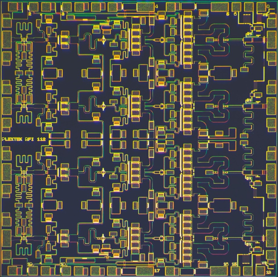
Figure 7. Die photograph of a PRFI 4-channel 28 GHz PA.
Four-channel, single-chip PAs
We have also designed a single-die, four-channel MMIC that covers the 28 GHz 5G band (see Figure 7). The ICs have been fabricated with Sanan IC’s P15EP process – a 4 V, 0.15 μm, enhancement-mode GaAs pHEMT process – and housed in a standard 5 mm by 5 mm plastic over-moulded QFN package. To benchmark performance, this package has been mounted on a representative evaluation PCB.
Each of the four PAs is a three-stage design that includes its own independent RF output power detector. For each channel, measured gain is 19.6 dB ±1.4 dB across 26 GHz to 29 GHz, and input and output return losses are 10 dB across the band. Although the PAs for 5G systems will be operated backed-off from compression, to provide a figure-of-merit to aid comparison, we have measured the RF output power at 1 dB gain compression. This gave a figure of 24.5 dBm, and a corresponding power-added efficiency of 19.5 percent. Values for saturated output power and corresponding power-added efficiency are 25.5 dBm and 21.5 percent.
If all four PAs are driven with coherent RF signals and deployed in a suitable four-element antenna array, the RF output signals will combine to provide an additional 6 dB in RF power over a single channel. By adjusting the phases of the signals to the four antenna elements, the direction of the beam can be steered electronically. As the gain of each antenna element also adds to the total effective isotropic radiated power, this approach increases the effective RF power and the range of the communications link.
The designs we have developed underpin the huge opportunity that the compound semiconductor industry has through the addition of millimetre-wave frequency bands to the 5G communications standard. Through innovation in device design, and careful selection of the packaging, there is much opportunity for market success.
Closing the Gap between Measured and Modelled MMIC Performance - PRFI White Paper: https://www.plextekrfi.com/wp-content/uploads/accurate_simulation_of_mmics.pdf
L. Devlin “A guide to SMT packaging of Microwave ICs” proceedings of the ARMMS RF and Microwave Society Conference, November 2012: https://www.plextekrfi.com/wp-content/uploads/Guide_to_ SMT_Packaging_of_Microwave_ICs.pdf


