
Researchers develop precision perovskite spray
New approach offers practical way to make multilayer perovskite solar cells
Although perovskites are a promising alternative to the silicon used to make most of today's solar cells, new manufacturing processes are needed to make them practical for commercial production. To help fill this gap, researchers have developed a new precision spray-coating method that enables more complex perovskite solar cell designs and could be scaled up for mass production.
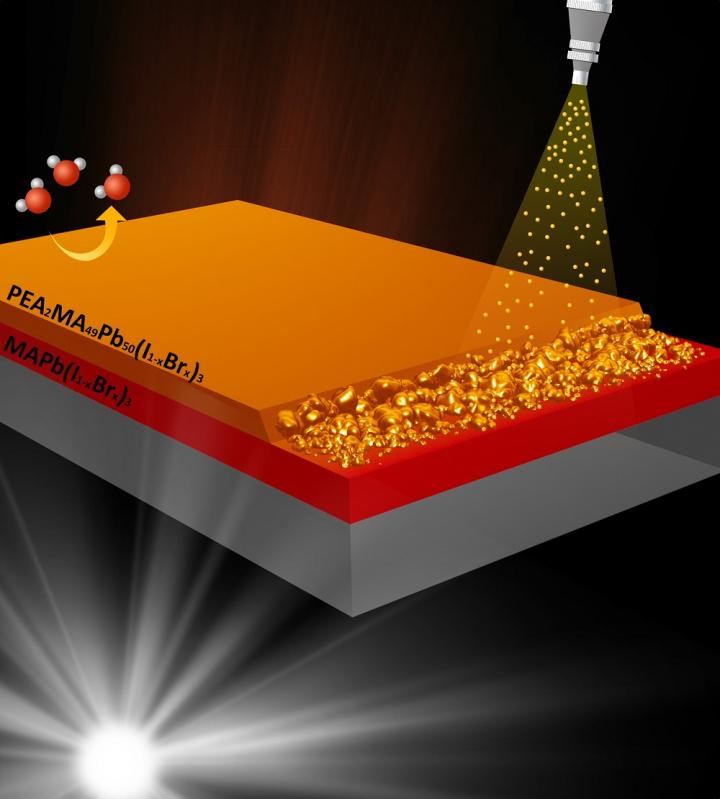
"Our work demonstrates a process to deposit perovskite layer by layer with controllable thicknesses and rates of deposition for each layer," said research team leader Pongsakorn Kanjanaboos from the School of Materials Science and Innovation, Faculty of Science, Mahidol University in Thailand. "This new method enables stacked designs for solar cells with better performance and stability."
In the Optical Society (OSA) journal Optical Materials Express, Kanjanaboos and colleagues describe their new spray coating method, called sequential spray deposition, and show that it can be used to create a multilayer perovskite design. Applying different perovskite materials in each layer can allow customisation of a device's function or the ability to meet specific performance and stability requirements.
A better way to spray
One of the advantages of perovskites are that they are solution processable, meaning that a solar cell is made by drying liquid perovskite into a solid at a low temperature. This fabrication process is much easier and less expensive than making a traditional silicon solar cell, a process that requires very high temperatures and cutting a solid material into wafers.
However, the solution process typically used to make perovskites does not allow multilayer designs because the upper layer tends to dissolve the already-dried lower layer. To overcome this challenge, the researchers turned to a process known as sequential spray deposition in which tiny droplets of a material are applied to a surface.
After trying different spray coating methods, they found one that worked at temperatures around 100degC. They then optimised the spray parameters to ensure that the tiny droplets dried and crystallised into solid perovskite immediately upon contact with the already-dried lower layer.
Building a multi-layer device
"With our spray coating process, the solution of the upper layer doesn't disturb the solid film making up the first layer," said Pongsakorn. "Endless combinations of stacked perovskite architectures with any number of layers can be designed and created with precise control of thicknesses and rates of deposition for each layer."
The researchers demonstrated the technique by depositing a perovskite material with high stability on different perovskite material with better electrical properties. This double-layer semi-transparent perovskite device showed clearly defined layers and simultaneously achieved high performance and good stability.
The researchers plan to use the new approach to make multilayer perovskite devices with new functions and combinations of performance and stability that were not possible before.
'Layer-by-layer spray coating of a stacked perovskite absorber for perovskite solar cells with better performance and stability under humid environment' by K. Amratisha et al; Opt. Mater. Express 10, 7, 1497-1508 (2020).


