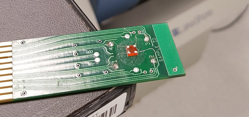
Vapour fix raises perovskite crystal performance

Hall measurements show that bromine vapour treatment enhanced the transport properties of hybrid perovskite crystals (orange)
A simple and noninvasive treatment could become a post-crystallisation process to optimise the optoelectronic properties of hybrid perovskite solar cell materials, according to researchers at KAUST (King Abdullah University of Science and Technology).
In this treatment, bromine vapours penetrate the surface of as-synthesised perovskite crystals to reach their deep-lying layers, removing surface and bulk defects generated during crystal growth.
Lead-containing hybrid perovskites, such as methylammonium lead tribromide (MAPbBr3), present unique charge transport properties and easy processability in solution. These make them attractive as potential low-cost alternatives to traditional silicon-based light-harvesting solar cell materials. However, approaches that use solution processing to crystallise them tend to leave contaminants, such as oxygen and amorphous carbon. These approaches also produce halide vacancies that create lead cations, which can trap electrons to form metallic lead and restrict charge transport.
Various chemical treatments can reduce these defects, but most tinker with the composition of the precursor solution to optimise thin film and crystal formation. However, the researchers from the KAUST Solar Center sought something simpler.
"We were interested in developing a facile recipe that could be applied once crystal formation was complete," says Ahmad Kirmani, now a postdoc at the National Renewable Energy Laboratory, U.S., who conducted the study under the supervision of Aram Amassian and Omar Mohammed.
Co-author Ahmed Mansour, now a postdoc at Helmholtz-Zentrum Berlin, Germany, describes how the researchers chose a bromine vapour treatment because they had previously observed the improved conductivity of graphene when exposed to bromine. "Bromine is a volatile liquid at room temperature and readily evapourates without the need for any external source of energy," Mansour says.
The researchers suspended MAPbBr3 crystals in a bromine-vapour-saturated environment and monitored the effects of bromine exposure on material properties.
They were pleasantly surprised to find that bromine vapours suppressed metallic lead on the surface as well as in the bulk of the crystals, Mohammed says. "This meant that we could access the bulk properties of these crystals, such as their electrical conductivity," he adds. Prolonged bromine exposure produced a dramatic 10,000-fold enhancement in bulk electrical conductivity and a 50-fold increase in carrier mobility. Further assessment revealed that perovskite crystallisation leaves behind voids and imperfections, which allows bromine to diffuse and permeate through the crystals.
Each of the former team members is currently exploring more applications for their treatment, such as for improving the power conversion efficiency of solar cells containing perovskite thin films as absorbers or for single-crystal devices--such as transistors, photodetectors and radiation detectors--that require excellent carrier mobility and intrinsic optoelectronic properties.
'Facile and noninvasive passivation, doping and chemical tuning of macroscopic hybrid perovskite crystals' by A.R Kirmani et al; PLoS ONE 15, e0230540 (2020)


