Loading...
News Article

Rena launches single wafer platform

News

Tool for clean, etch, strip and dry processes enables the transition from R&D to pilot production

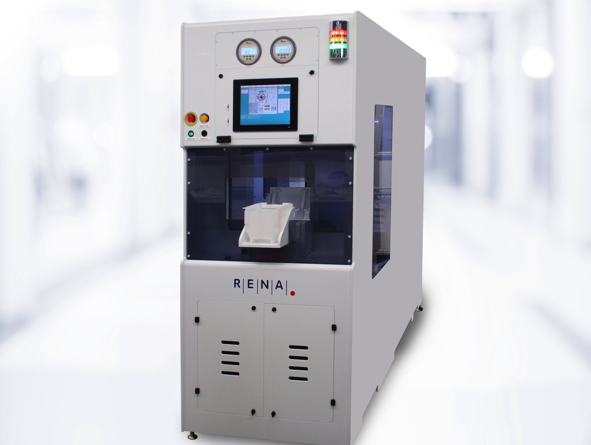
Rena Technologies, a company known for immersion and batch spray technology, has added a single wafer platform for semiconductor processing to its portfolio. Called Inception, the new tool enables transition from R&D to pilot line production, and is capable of all semiconductor wet processes like clean, etch, strip and dry.

The first Inception single wafer tool has already been shipped to a major compound semiconductor customer who will use its capabilities in an acid clean process.

Ed Jean, CEO of Rena Technologies says: “if all you have is a hammer, everything looks like a nail, Batch Immersion, batch Spray, and single wafer tools all have their place in the wet process world. Most equipment suppliers however offer a one-size-fits-all approach, trying to 'hammer' your application into the only platform they offer. With the addition of the Inception single wafer tool to our product lineup, Rena provides the appropriate platform for any wet clean, etch, or strip application.”

Heath Phillips, Rena Technologies spray product manager says: “The Inception single wafer platform provides our customers, who perform tests in beakers and pie plates, the consistency to develop a process of record and automate their process.”

Features of the Inception single wafer tool include: FEoL (Acid) & BEoL (Solvent) processing applications; automated wafer handling (manual load optional); wafers up to 200 mm and masks up to 7 x 7; dual moving spray arms with separate chem lines; stationary bottom spray nozzles for DI and N2; etch uniformity exceeds batch systems; standard dual tank design provides multi-step processing (4-tank optional); single or dual load ports; low utilities consumption; and a small footprint

SiC MOSFETs: Understanding the benefits of plasma nitridation
Wolfspeed reports Q2 results
VueReal secures $40.5m to scale MicroSolid printing
Mitsubishi joins Horizon Europe's FLAGCHIP project
Vishay launches new high voltage SiC diodes
UK team leads diamond-FET breakthrough
GaN adoption at tipping point, says Infineon
BluGlass files tuneable GaN laser patents
QD company Quantum Science expands into new facility
Innoscience files lawsuit against Infineon
Riber revenues up 5% to €41.2m
Forvia Hella to use CoolSiC for next generation charging
Photon Design to exhibit QD simulation tool
Ortel transfers CW laser fabrication to Canada
Luminus adds red and blue multi-mode Lasers
PseudolithIC raises $6M for heterogeneous chiplet tech
Mesa sidewall design improves HV DUV LEDs
IQE revenue to exceed expectations
'Game-changing' VCSEL system targets clinical imaging
German start-up secures finance for SiC processing tech
Macom signs preliminaries for CHIPS Act funding
IQE and Quintessent partner on QD lasers for AI
EU funds perovskite tandems for fuel-free space propulsion
EU to invest €3m in GeSi quantum project
Transforming the current density of AlN Schottky barrier diodes
Turbocharging the GaN MOSFET with a HfO₂ gate
Wolfspeed launches Gen 4 SiC MOSFET technology
Report predicts high growth for UK's North East
Element Six unveils Cu-diamond composite
SemiQ launches hi-rel 1700V SiC MOSFETs
Lynred to exhibit Eyesential SWIR sensor for machine vision
Thorlabs buys VCSEL firm Praevium Research
×
Search the news archive

To close this popup you can press escape or click the close icon.
Logo
x
Logo
×
Register - Step 1

You may choose to subscribe to the Compound Semiconductor Magazine, the Compound Semiconductor Newsletter, or both. You may also request additional information if required, before submitting your application.


Please subscribe me to:


You chose the industry type of "Other"

Please enter the industry that you work in: