
BAE and AFRL program accelerates GaN radar development
Collaboration with Air Force Research Laboratory accelerates development of next-generation radar, electronic warfare, and communications technology
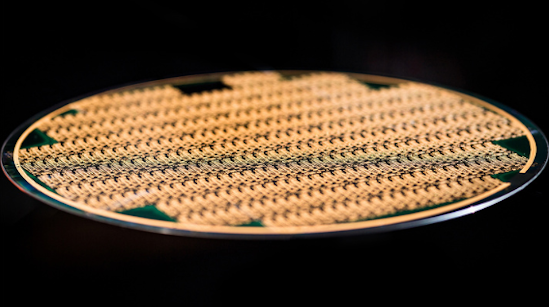
BAE Systems’ FAST Labs research and development organisation continues to advance millimetre wave GaN semiconductor technology to support critical next-generation radar, electronic warfare, and communications. It is currently in Phase 3 of a multi-year, cooperative agreement with the Air Force Research Laboratory (AFRL), developing defence-critical GaN technologies .
In particular, GaN technology fills a unique DoD need for low-cost, high-performance amplifier technology.
In this multi-phase program, Phase 1 focused on transitioning the technology to BAE's foundry from AFRL, Phase 2 is about maturing the technology and scaling to 6-inch wafers to slash per-chip costs. Phase 3, which runs concurrently with Phase 2, extends this technology and for the first time, provides technology access to a larger community to develop high-performance integrated circuits for next-generation applications. Developing this expertise and capability onshore is part of the DoD’s ongoing effort to build a trusted, US-based supply of key advanced electronics capabilities.
Phase 3, includes a government sponsored challenge – using BAE Systems' foundry and expertise – that will open access to non-traditional teams from industry and universities to gain design diversity and experience in GaN across the broader community. Expanding the universe of organisations that can access GaN and develop applications using the technology could exponentially speed adoption of this key technology.
“This GaN program with AFRL is establishing the foundation for advanced technology development that could lead to new mission critical technologies for a generation of warfighters,” said Chris Rappa, product line director for Radio Frequency, Electronic Warfare, and Advanced Electronics at BAE Systems FAST Labs. "As a result of this multi-year, multi-phase program and our own internal investment, we have seen more than $15 million worth of updates to technology and facilities that will allow additional growth, and increased capacity to help fulfil the DoD’s goal of creating additional trusted, U.S.-based centers of excellence for next-generation technology.”
The GaN program is part of BAE Systems’ defence electronics research and development portfolio, its open foundry service, and builds on the success of its recently announced T-MUSIC award, and MATRICs technology. BAE Systems is researching and advancing world-class microelectronic technologies, including GaN, in a 70,000-square-foot Microelectronics Center (MEC) located in Nashua, New Hampshire. The MEC has been an accredited DoD Category 1A Trusted Supplier since 2008, and fabricates integrated circuits in production quantities for critical DoD programs.


