
Major breakthroughs for the fabrication of ultrasmall, ultracompact, ultrahigh efficient InGaN μLEDs
Professor Tao Wang and his team at The University of Sheffield have achieved record efficiency and a record spectral linewidth for the fabrication of ultra-small μLEDs.
There is a significant growing interest in developing III-nitride microLEDs (μLEDs), the key components for microdisplays which are crucial for smart phones, smart watches, AR and VR devices. These kinds of devices require μLEDs with an ultrasmall diameter (≤5 μm), high external quantum efficiency (EQE), and narrow spectral line width.
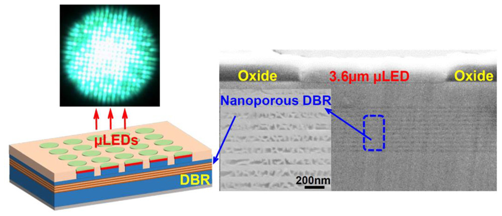
The μLEDs with a diameter down to 3.6 μm and an interpitch down to 2 μm exhibit an ultrahigh maximum EQE of around 9%, which is 50% higher than those of the μLEDs without distributed Bragg reflectors (DBRs). More importantly, the spectral line width has been significantly reduced down to 25 nm, which is the narrowest value reported so far for III-nitride green μLEDs.
Dry etching, which is currently the most crucial step for the fabrication of μLEDs introduces severe damage, which seem to become an insurmountable challenge for achieving ultrasmall μLEDs with high EQE. Furthermore, it is well-known that μLEDs which require InGaN layers as an emitting region naturally exhibit significantly broad spectral line width, which becomes increasingly severe toward long wavelengths such as green.
The research team identified the key to the success of the approach is due to the utilization of a direct epitaxial growth on a prepatterned template, which does not involve any dry-etching process, and thus eliminates any resultant etching damage.
Their strategy is to combine the lattice-matched DBRs and selective overgrowth method. This is used as a template for further SiO2 microhole array patterning on top. SiO2 film with a thickness of 500 nm is deposited on the template by means of employing a standard plasma-enhanced chemical vapor deposition (PECVD) technique. Afterwards, standard photolithography and drying etching techniques are used to selectively etch the dielectric layer down to the n-type GaN surface, forming regularly arrayed microholes with a diameter of 3.6 μm and an interpitch of 2 μm.
Next, a standard InGaN-based LED structure is selectively grown on such a patterned template by a standard metalorganic vapor phase epitaxy (MOVPE) technique.
Because of the dielectric masks, the growth of the LED structure is restricted within the microholes, leading to the natural formation of μLED arrays. The physical parameters are fully determined by the SiO2 microhole masks, meaning that the formation of μLED arrays does not involve any μLED mesa etching processes.
In order to clearly demonstrate emitting μLED pixels, its micro-electroluminescence (EL) measurement system has been employed to record microscopy images. A LCS-100 characterization system is used to measure both light outputs and EQE on their bare-chip LEDs in a CW mode, where the system is equipped with an integrating sphere system and a CCD APRAR spectrometer.
Further enhancement in EQE is still required for high performance microdisplays and the intrinsically broad spectral line width of μLEDs will have to be significantly reduced. The Centre for GaN Materials and Devices in Sheffield continues to develop cutting-edge technologies and perform advanced research on III-nitride materials and devices.
Ultrasmall, Ultracompact and Ultrahigh Efficient InGaN Micro Light Emitting Diodes (μLEDs) with Narrow Spectral Line Width, Jie Bai, Yuefei Cai, Peng Feng, Peter Fletcher, Chenqi Zhu, Ye Tian, and Tao Wang, ACS Nano 2020, 14, 6, 6906–6911, 2020


