

Six-junction super cells

Increasing the junction count to six propels solar efficiency to a new high and provides a pathway to smashing the 50 percent barrier
BY RICHARD STEVENSON
THERE ARE TWO large levers pulled by every developer of high-efficiency solar cells. One is adding more junctions, as this allows the energy that is absorbed by the sun to be put to better use; and the other is to concentrate the sunlight, using mirrors or lenses. But to realise really high efficiencies, the quality of the design and its execution must be first rate.
Those that set a new benchmark for solar efficiency tend to combine hard-won expertise with a great design. This is evident in the record-breaking, innovative six-junction cell reported recently by John Geisz and co-workers from the National Renewable Energy Laboratory (NREL) in Golden, Colorado. The efficiency of their device exceeds 47 percent, and it could eclipse 50 percent by addressing a relatively high resistance.
This team’s triumph draws on decades of progress in multi-junction cells, which first hit the headlines in the mid-1990s when cells with two junctions started to outpace single-junction rivals. In the decade that followed, further progress came from a three-junction variant, initially made by forming a germanium cell on a germanium substrate and adding sub-cells from the likes of InGaAs and GaInP. A team at NREL, working with engineers from the US-firm Spectrolab, made much progress on this front, reporting an efficiency of around 32 percent in November 1999. Refinements to this design, by both this collaboration and others, provided a pathway towards 40 percent.
Although this approach takes efficiency well beyond that realised with the very best single-junction cell, it only gets you so far. Part of the issue is that the design restricts the choice of bandgaps to those lattice-matched to the substrate, in order to maintain crystal quality. If an optimal set of bandgaps cannot be applied, efficiency is compromised. Another impediment is that while the use of germanium is convenient, allowing the bottom junction to be made from the same material as the substrate, it’s not the best choice. Due to its indirect nature, efficiency lags that of the III-Vs. The latter also benefit from the insertion of III-V heterojunctions, which provide passivation and eradicate energy-sapping minority carrier recombination at the interfaces.
To overcome all these limitations associated with a germanium bottom junction, in the ‘noughties’ researchers from NREL pioneered an inverted metamorphic design. It features a reversing of the growth order of the cells. Growth begins with two high-energy sub-cells that are lattice-matched to a GaAs substrate, before the lattice constant is changed with a grading structure, prior to the addition of a third, lower-energy cell. Substrate removal follows after the device is flipped, allowing light to enter the device through the sub-cell with the highest energy. The upshot is that by inverting the order of growth, two cells are lattice matched to the substrate, rather than one, leading to improved material quality for the device and ultimately the potential for a higher efficiency. Many groups adopted this new triple-junction architecture, with competition driving up efficiency from just below 40 percent to significantly above it.
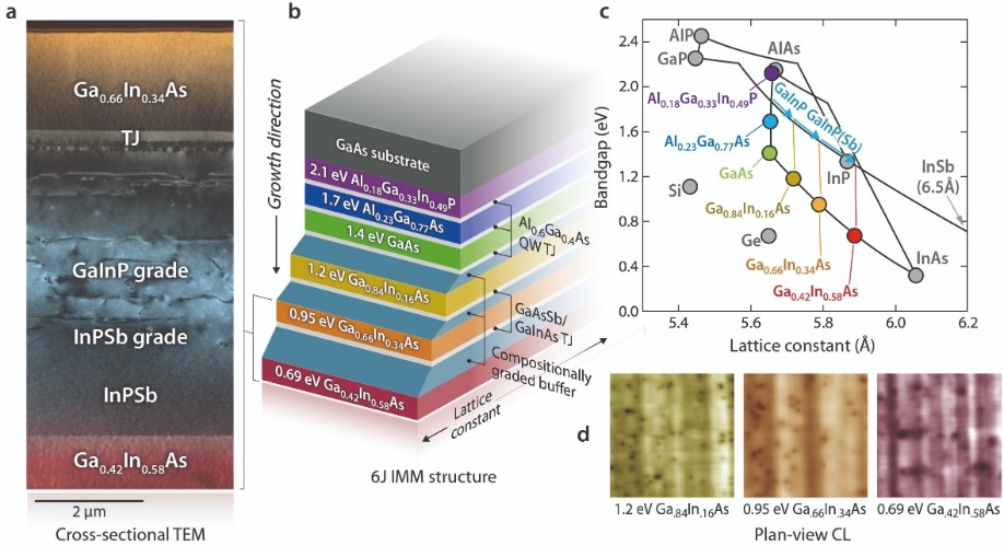
Figure 1: Researchers at NREL have produced a six-junction solar cell with record-breaking efficiency. The inverted metamorphic design features GaInP and InPSb grading layers (a), a variety of tunnel junctions (b), and the use of sub-cells with differing lattice constants (c). Scrutinising material quality with cathodoluminescence (d) revealed that threading dislocation densities are as low as around 106 cm-2 in each sub cell. Under one sun operation, the open-circuit voltage for the six-junction cell is 5.55 V, while the fill factor is 83.5 percent and the short-circuit current density is 8.46 mA cm-2. At 143 suns, the concentration that provides the highest efficiency, the open-circuit voltage increases to 6.29 V, the fill factor climbs to 87.2 percent and the short-circuit current density hits 1.23 A cm-2. Taken from Nature Energy J. Geisz et al. https://doi.org/10.1038/s41560-020-0598-5
In the last decade, some radical designs have taken the efficiency even higher. In late 2010 Spire Semiconductor grabbed the record with a device that had cells on both sides of the substrate. Operating at 406 suns, it had an efficiency of just over 42 percent. To better this, US Start-up Solar Junction used a lattice-matched device with a new feature – a dilute nitride for the bottom junction. In April 2011 they raised the bar to 43.5 percent efficiency, realised at 418 suns, before making further headway, reporting 44 percent in October 2012, for a device operating at 947 suns.In the summer of 2013 the triple-junction inverted meta-morphic cell briefly regained pole position. Success came from Sharp, producing a 44.4 percent efficient device at 302 suns.
From then on, record-breaking cells have had at least four junctions. French firm Soitec took the record from Solar Junction by drawing on expertise in wafer bonding. By uniting a pair of two-junction devices, designers could exploit far greater freedom in their choice of lattice constants for the cells. Refining this technology in partnership with researchers at the Fraunhofer Institute for Solar-Energy Systems, Germany, yielded a cell with 46 percent efficiency. Reported in late 2014, this record has stood for far, far longer than its predecessors.
Six-junction successes
To break this record, Geisz and co-workers have returned to the inverted metamorphic design, but upped the number of junctions to six. Helping their success has been their previous work on a four-junction device, formed by replacing a single InGaAs cell with a pair of them. This modification produced an efficiency of 45.6 percent at 690 suns, just below the record realised with the wafer-bonded cell.
Although Geisz has had much success with the inverted metamorphic over many years, he is not dismissive of alternative approaches. He views the dilute nitrides as very promising but challenging, having spent much time at around the turn of the millennia trying to make high-performance devices that incorporated this material system. However, he never enjoyed significant success with dilute nitrides. “At least by MOCVD, we haven’t been able to get as good a quality as we have with the metamorphic InGaAs. Solar Junction had a lot of good success, but they were growing that by MBE.”
The other approach that has produced record-breaking cells in recent times, wafer bonding, also has much merit, according to Geisz. “When we started the six-junction project, wafer bonding was one of the avenues that we would have liked to investigate. It’s really promising.”
But there is a price to pay for the freedom of design associated with wafer-bonding – relatively high costs, resulting from the need for twice as many growths and twice as many substrates.
Having started with an inverted metamorphic with three junctions and then moved on to designs with four, it may seem that progressing to five would be the logical way forward. But it’s not, argues Geisz: “We got the most bang for our buck working on six junctions directly. The six junction is kind of a natural sweet spot.”
Fabrication of NREL’s record-breaking cells began by loading GaAs substrates into an MOCVD chamber and growing 140 layers. This takes about seven-and-a-half hours, compared with just 3 hours for the original three-junction variant that has about 60 layers. Note that MOCVD is preferred to the other common approach for depositing these layers, MBE, because the growth recipe scales well, growth rates are higher, and it is easier to introduce sources into the chamber for all the layers and their dopants.
Growth of the six-junction structure begins with lattice-matched cells of Al0.18Ga0.33In0.49P (2.1 eV) and Al0.23Ga0.77As
(1.7 eV). They replace the single GaInP cell found in a three- or four-junction device. After that comes GaAs, the only binary cell. “It’s really a good material, so whenever possible, we like to use gallium arsenide”, explains Geisz.
The most radical change comes next. Rather than using just a single junction to collect all the low-energy photons, three are employed, separated by compositionally graded buffers. The justification for this, according to Geisz, is that there is a significant proportion of the sun’s radiation in the infra-red region.
To produce the buffers between the three cells – they are made of Ga0.84In0.16As (1.2 eV), Ga0.68In0.34As (0.95 eV), and Ga0.42In0.58As (0.69 eV) – metamorphic concepts are pushed to the limit. “We are grading it out beyond the lattice constant of indium phosphide,” says Geisz. “We’re using about 4.2 percent lattice mismatch.”
Buffers: arsenides vs phosphides
When Geisz and his co-workers started developing their six-junction cells, they used AlGaInAs for the grading layers. More recently, they have switched to GaInP, which yields better properties for the bottom junctions.
“Using phosphides is expensive and hard on the reactors,” warns Geisz, but he says that this must be weighed against their good properties. “The ordering in gallium indium phosphide tends to stabilise phase separation, and give some preferential glide to the dislocations.”
Due to this, dislocations are confined to the inactive regions, boosting efficiency. Benefits are seen when scrutinising the material with transmission electron microscopy and cathodoluminescence, techniques revealing that the typical threading dislocation density in the sub cell is 106 cm-2.
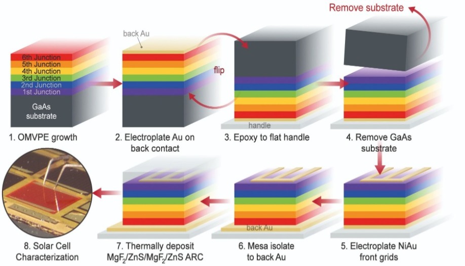
Figure 2: Fabrication of the six-junction solar cell begins with the epitaxial growth of a semiconductor stack, and then the deposition of a gold film. After bonding this gold layer to a handle substrate, the substrate is removed, before adding grids and an anti-reflection coating. Taken from J. Geisz et al. Nature Energy https://doi.org/10.1038/s41560-020-0598-5
Like other multi-junction cells, tunnel-junctions provide electrical connections between the sub-cells. The combination of Al0.6Ga0.4As layers and GaAs quantum wells are used for the first three tunnel junctions to ensure transparency, but this is not suitable for the last two. When connecting the metamorphic cells, the team developed metamorphic tunnel junctions, made of carbon-doped GaAsSb and selenium-doped GaInAs.Measurements on NREL’s record-breaking six-junction devices show that efficiency peaks at 47.1 percent at 143 suns. At higher concentrations, reductions are modest, dropping to a still impressive 44.9 percent at 1,116 suns. By tweaking the design, Geisz and co-workers also produced a device for maximum efficiency at 1 sun. Featuring a third sub-cell made from Al0.03Ga0.97As rather than GaAs, it produced an efficiency of 39.2 percent. Although that’s better than the previous high of 38.8 percent for a five-junction bonded cell, it does not make it into the record books, as qualification requires a minimum size for the cell of 1 cm by 1 cm.
While the obvious fit for this six-junction photovoltaic is at the heart of a concentrating system that sets new benchmarks for efficiency and power generation per unit area, it is also a very attractive candidate in unmanned aerial vehicles, where its excellent power-to-weight ratio is a massive asset.
Another market for the multi-junction cell is in space, generating power for satellites. To ensure that the latest NREL device performed at its best in this application, modifications would be required to the compositions and thickness of all six cells. But even if those changes were optimised, there would still be concerns related to radiation hardness.
“In general, the arsenides are not as radiation hard as the phosphide materials,” says Geisz, who has used a ternary arsenide, InGaAs, in the metamorphic junctions of the team’s record-breaking cells.
To see if this could be a show-stopper, the researchers are now starting to look into radiation hardness issues. “It’s not clear what the biggest issue for radiation hardness is,” admits Geisz, who says that investigations will begin by considering the impact of dislocations in the device.
Another goal for the team is to trim the resistance of their six-junction cell. It’s currently around ten times that of its three- and four-junction cousins, due to more pronounced zinc diffusion, resulting from longer growth times and higher growth temperatures; and the relatively high proportion of aluminium in the top sub-cell, which reduces carrier mobility, leading to an increase in resistance between the grids.
Hitting 50 percent
If the resistance of the six-junction design could be reduced to around 0.15 Ω cm2, the value realised in cells with fewer junctions, efficiency should increase to beyond 50 percent. In addition, the peak of the efficiency should shift to a higher concentration. This means that even without increasing material quality, efficiency could exceed 50 percent at 1000 suns.
The combination of record-breaking efficiency and a clear pathway to even better performance will pique the interest of makers of multi-junction cells all over the world. Fortunately, NREL is very open to working with cell manufacturers.
“We have been pretty straightforward about putting the technology into open literature, so we are hopeful someone will use it,” says Geisz. “We are funded by the US Department of Energy and we are looking to develop this technology for the good of all.”
While exceeding an efficiency of 50 percent would be a substantial milestone for a multi-junction cell, it’s by no means the limit of what may be possible. Even conservative calculations suggest that the upper bound for efficiency is as high as 62 percent, realised with a concentration of 1000 suns.
Closing in on this is by no means the only target for the team. One of its near-term goals is to bring down the cost of these devices, so III-V solar cells can compete with silicon technology. This is a substantial challenge, but the inverted metamorphic has the upper hand in one regard – it allows re-use of the substrate, a promising option for cutting material costs. “We are also looking at simplifying the very high efficiency structures,” adds Geisz, explaining that this offers another route to making high efficiencies more affordable.
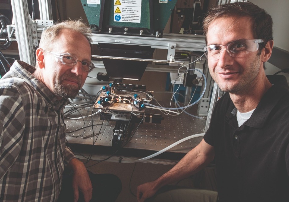
Efforts at developing a six-junction cell at the NREL in Golden, CO, have been led by John Geisz (left), Principle Scientist in the High Efficiency Crystalline Photovoltaics Group. A key member of the team is Ryan France (right).
Credit: Dennis Schroeder, NREL.
Attempts to simplify structures could lead to fewer junctions. “It seems like six junctions is a lot, and we may wish to back off on that,” says Geisz. So don’t expect NREL to be reporting a record-breaking seven or eight junction cell in a year or two. “Never say never, but it seems like six junctions is as high as practical.”


