
Banishing the buffer

Buffer-free GaN-on-SiC epiwafers enable cost-competitive, higher performance power devices
BY JR-TAI CHEN FROM SWEGAN AB
2020 is the year of the GaN power device. Following several decades of intensive research and development in both materials and devices, GaN-on-silicon HEMTs are starting to make inroads into the mainstream consumer market. One example is the shipment of more than one million units of ultra-fast portable GaN chargers for mobile phones.
While these substantial orders are a triumph, there is an opportunity for significant further improvement. GaN-on-silicon HEMTs are failing to operate close to electric field strengths promised by this wide bandgap material, and that shortfall is holding back performance on many fronts, including operating voltages, device miniaturisation and on-resistance, which has the potential to fall by an order of magnitude. The good news is that such progress is within the grasp of the entire power electronics industry. All that is needed is to move to a recently developed, buffer-free GaN-on-SiC material known as QuanFINE, which has been developed by our team at SweGaN AB in Linköping, Sweden.
We have been developing this material for several years. Back in 2018, we demonstrated the world’s first high-quality, high-performance, buffer-free GaN-on-SiC HEMT. This features a revolutionary epitaxial stack, which is free from the conventional thick carbon-doped buffers that are used in high-voltage GaN-on-silicon based HEMTs – and also, for that matter, GaN-on-SiC HEMTs used for RF applications. By removing the buffer that is at least 5 µm thick and a drift layer of comparable thickness, device production costs fall and reactor up-time increases, thanks to a reduced cleaning frequency for the MOCVD chamber.
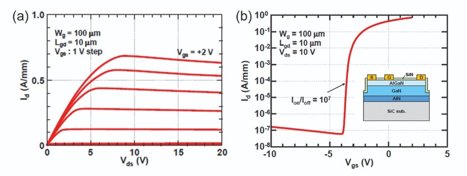
Figure 1. (a) DC plots of the drain current as a function of drain-source voltage (a) and gate-source voltage (b) for a power HEMT produced with SweGaN’s buffer-free GaN-on-SiC technology.
Armed with our technology, the total epitaxial layer thickness of GaN-on-SiC heterostructures is below 350 nm, a feat accomplished without any compromise in material properties. At the heart of our buffer-free, GaN-on-SiC heterostructure is a completely new growth mechanism: transmorphic heteroepitaxy. Its distinctive feature is that there is no abrupt change in either the composition or the atomic configuration at the material interface. Instead, there is a gradual transition from one to the other over a nanometre, occurring via vacancy ordering.The success of our material hinges on its capability to withstand a high electrical breakdown field. According to theory, the critical breakdown field of GaN is approximately 3 MV/cm. We are not far from that upper limit, with a recent study based on a two-terminal lateral breakdown test showing our material can handle close to 2 MV/cm. That figure, obtained on a structure featuring a 200 nm-thick GaN channel layer, a 60 nm AlN nucleation layer and no field plates, is far higher than that for GaN-on-silicon devices with a carbon-doped buffer – for that class of HEMT, even with the benefit of field plates, the breakdown electrical field is typically 0.6-0.7 MV/cm.
Device testing
To further explore the potential of our buffer-free technology for power applications, we have collaborated with the research group at the University of Fukui, Japan, led by Masaaki Kuzuhara and Joel Asubar. This team, which has been developing techniques to increase the breakdown strength of GaN HEMTs for many years, have previously used low-dislocation-density, iron-doped GaN substrates to propel the breakdown field to 1 MV/cm. These devices reach a breakdown voltage of 5 kV.
Our collaborative effort has involved undertaking breakdown tests on buffer-free HEMTs that have a nominal 25 nm Al0.25Ga0.75N barrier and a 250 nm GaN channel layer. These transistors, fabricated using standard technology developed by the University of Fukui, have a 3 µm gate length, a gate-to-source spacing of 3 µm, a 200 nm mesa isolation depth and a SiN passivation layer 150 nm-thick (see the inset of Fig. 1(b) for details of the device configuration).
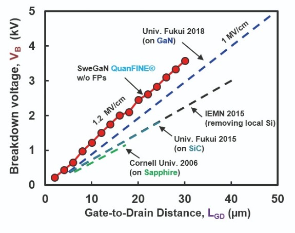
Figure 2. Benchmarking the breakdown voltage at different gate-to-drain distances for GaN HEMT power devices based on different epitaxial growths. Some data comes from J, Asubar et al. “Pushing the GaN HEMT Towards Its Theoretical Limit,” Compound Semiconductor, October 2016, pp. 26-31. In addition, there are results associated with a buffer-free epiwafer measured in this work.
DC current-voltage measurements on these buffer-free HEMTs reveal that they have a reasonable current density (see Figure 1(a)) and a remarkably low leakage current (see Figure 2(b)) that leads to an Ion/Ioff ratio of 107. Note that the entire epitaxial structure is unintentionally doped. The low leakage current is testament to the high-quality, ultra-wide bandgap AlN nucleation layer that provides a back barrier.Breakdown tests on a range of our devices, with gate-to-drain distances varying from 0.2 µm to 30 µm, have enabled benchmarking of the critical field strength with state-of-the-art values for GaN grown on different substrates (see Figure 2). As one would expect, the breakdown voltage of our HEMTs increases in a linear manner with the gate-to-drain distance, reaching 3.6 kV at a distance of 30 µm. This translates to a field strength of 1.2 MV/cm, a value higher than that for GaN HEMTs grown on native substrates. Such an impressive result validates the high structural quality of our buffer-free epiwafers, and the effectiveness of using an AlN nucleation layer and a semi-insulating SiC substrate to block high voltages.
Eagle-eyed readers will have spotted that the breakdown field strength for our HEMTs is lower than that recorded for the two-terminal measurement. This discrepancy might result from differences in the methods used to create device isolation. For the two-terminal measurement, a nitrogen ion-implantation provided isolation; and for the HEMTs this resulted from the mesa. We are planning an additional investigation, targeting further optimisation of our buffer-free HEMTs, so that they offer a better breakdown performance.
To put our value for field strength in perspective, the figure of 1.2 MV/cm is four times that for equivalent, commercial, field-plate-free GaN-on-silicon HEMTs (see Table 1). These results show that our buffer-free technology has the potential to reach a lateral breakdown voltage of about 5 kV with standard GaN power device designs.
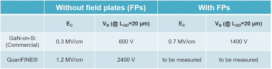
Table. 1. A comparison of the critical electric field strength, Ec, and the breakdown voltage (VB) for commercial GaN-on-silicon epiwafers and those made by SweGaN, featuring buffer-free technology. Measurements are reported for devices with and without field plates. Note that field plates are commonly used in GaN HEMTs to enhance breakdown voltage. In most cases field plates enhance the magnitude of the electric field strength and the breakdown voltage more than two-fold.
Another opportunity that is created with our technology is to shrink device dimensions while retaining the voltage rating of commercial GaN-on-silicon devices. For example, by switching from GaN-on-silicon material to our buffer-free technology, it is possible to trim the gate-to-drain spacing in 600 V GaN power devices without field plates from 20 µm to 5 µm. This miniaturisation would result in a significantly reduced power loss. According Baliga’s figure-of-merit, on-resistance is inversely proportional to the cube of the critical electric field strength, so a HEMT made with our technology should exhibit an on-resistance that is 1/64th that for an equivalent GaN-on-silicon device with the same voltage rating.Building on these benchmark results, and in preparation to enter the GaN power market, we have expanded our portfolio of products from 75 mm and 100 mm epiwafers to include those with a 150 mm diameter. Progress with the latter has led to a highly uniform growth process, and deliveries of this new product to customers in the first quarter of this year.
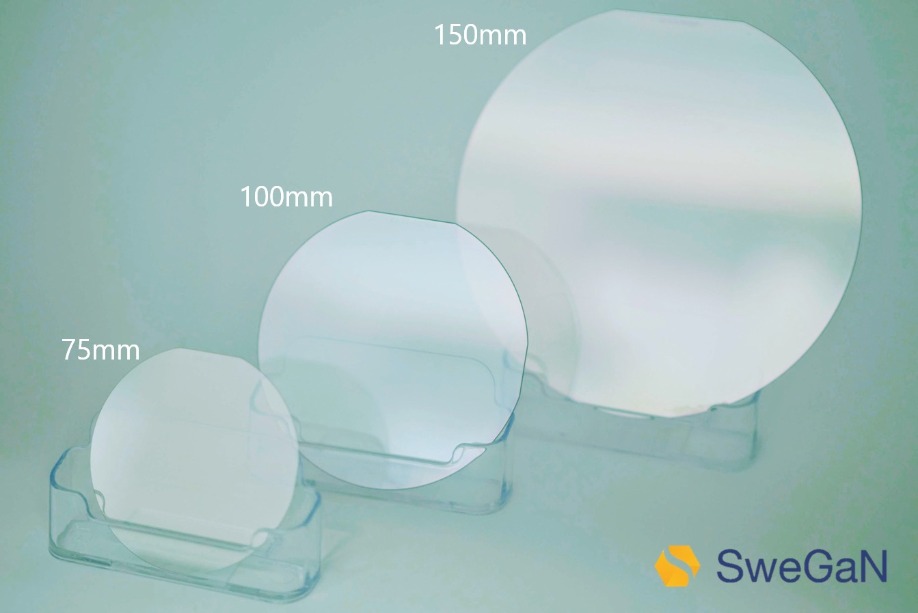
Figure 3. SweGaN’s product portfolio of buffer-free GaN-on-SiC epiwafers.
As we grow our business, we are well-positioned to benefit from steadily increasing in orders within the power industry for 150 mm semi-insulating SiC substrates, and the increasing volume by suppliers meeting this demand. The price of 150 mm semi-insulating SiC is expected to fall, aligning with the price of 150 mm n-type SiC wafers. This will enable our technology to become even more competitive.We are targeting the markets where device performance and reliability are the top priorities for customers and end users. As volumes increases for wide bandgap power electronics, material costs will naturally fall through economies of scale, creating a vast opportunity for our buffer-free technology in the cost-sensitive power market.
Our technology is also destined to enjoy success in the RF device industry. It has already attracted the attention of the majority of GaN RF foundries worldwide, and we expect that it will not be long before it is used in RF device production.
The ECSEL Joint Undertaking (JU) under grant agreement No 826392, UltimateGaN.
J.-T. Chen et al. Appl. Phys. Lett. 113 041605 (2018)
J. Lu et al Appl. Phys. Lett. 115 221601 (2019)
J, Asubar et al. “Pushing the GaN HEMT Towards its Theoretical Limit,” Compound Semiconductor, October 2016, pp. 26-31.


