

Electrons in the fast lane
Microscopic structures could further improve perovskite solar cells
Solar cells based on perovskite compounds could soon make electricity generation from sunlight even more efficient and cheaper. The laboratory efficiency of these perovskite solar cells already exceeds that of the well-known silicon solar cells. An international team led by Stefan Weber from the Max Planck Institute for Polymer Research in Mainz has found microscopic structures in perovskite crystals that can guide the charge transport in the solar cell. Clever alignment of these electron highways could make perovskite solar cells even more powerful.
When solar cells convert sunlight into electricity, the electrons of the material inside the cell absorb the energy of the light. Traditionally, this light-absorbing material is silicon, but perovskites could prove to be a cheaper alternative. The electrons excited by the sunlight are collected by special contacts on the top and bottom of the cell. However, if the electrons remain in the material for too long, they can lose their energy again. To minimise losses, they should therefore reach the contacts as quickly as possible.
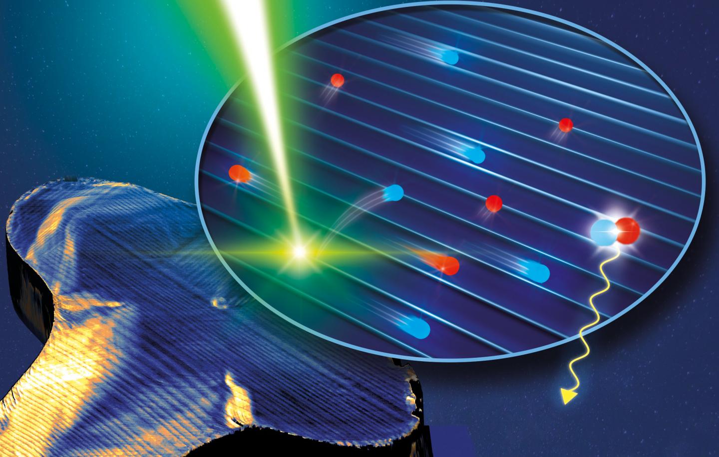
Microscopically small structures in the perovskites - so-called ferroelastic twin domains - could be helpful in this respect: They can influence how fast the electrons move. An international research group led by Stefan Weber at the Max Planck Institute for Polymer Research in Mainz discovered this phenomenon. The stripe-shaped structures that the scientists investigated form spontaneously during the fabrication of the perovskite by mechanical stress in the material. By combining two microscopy methods, the researchers were able to show that electrons move much faster parallel to the stripes than perpendicular to them. "The domains act as tiny highways for electrons," compares Stefan Weber.
Possible applications in LEDs radiation detectors
For their experiments, the researchers first had to visualise the stripe-shaped domains. They succeeded in doing this with a piezo force microscope (PFM). Five years ago, Weber and his colleagues discovered the domains for the first time in a perovskite crystal using this method. "Back then, we already wondered whether the structures had an influence on the operation of a perovskite solar cell," Weber explains. "Our latest results now show that this is the case."
The breakthrough came when the researchers compared their PFM images with data obtained from another method called photoluminescence microscopy. "Our photoluminescence detector works like a speed trap," explains Ilka Hermes, researcher in Weber's group and first author of the study. "We use it to measure the speed of electrons in different directions at the microscopic level." Hermes discovered that along the stripes the electrons moved about 50 to 60 percent faster than perpendicular to them. "If we were able to make the stripes point directly to the electrodes, a perovskite solar cell could become much more efficient", concludes Hermes.
With the new results, not only solar cells could be improved. Other optoelectronic applications such as light-emitting diodes or radiation detectors could also benefit from directed charge transport. "In general, it is an advantage if we can direct the electrons in the right direction," explains Stefan Weber. The researchers' idea: to put perovskite crystals under mechanical stress during their production. This so-called strain engineering would enable an optimised orientation of the electron highways.
'Weber Anisotropic carrier diffusion in single MAPbI3 grains correlates to their twin domains' by Ilka M. Hermes et al; Energy & Environmental Science 2020